DLPU132A October   2023  – March 2024 DLPC964


  1.   1
  2.   Description
  3.   Get Started
  4.   Features
  5.   Applications
  6.   6
  7. 1Evaluation Module Overview
    1. 1.1 Introduction
    2. 1.2 Kit Contents
    3. 1.3 Specification
    4. 1.4 Device Information
  8. 2Hardware
    1. 2.1 DLPLCRC964EVM Power Supply Requirements
      1. 2.1.1 External Power Supply Requirements
    2. 2.2 DLPLCRC964EVM Connections
      1. 2.2.1  J1, J2 - HPC FMC Connector (Male)
      2. 2.2.2  J3 - Input Power
      3. 2.2.3  J4 - TestMux Connector
      4. 2.2.4  J6, J8 - I2C Address Selectors
      5. 2.2.5  J7 - JTAG Boundary Scan
      6. 2.2.6  J9 - Micro-B USB Connector
      7. 2.2.7  J10 - I2C Connector
      8. 2.2.8  J11 - 3.3V GPIO Connector
      9. 2.2.9  J12 - 1.8V GPIO Connector
      10. 2.2.10 J13, J14, J15, J16 - DMD EVM Board Flex Cable Connectors
      11. 2.2.11 J17 - DMD_DMux Connector
      12. 2.2.12 J18 - FanSink Connector
      13. 2.2.13 Switches
        1. 2.2.13.1 SW1 - DMD park (PARK_Z)
        2. 2.2.13.2 SW2 - DLPC964 Reset
      14. 2.2.14 DLP LightCrafter DLPC964 LEDs
        1. 2.2.14.1 DLPLCRC964EVM Power and Status LEDs
    3. 2.3 EVM Assembly
      1. 2.3.1 DLPLCRC964EVM and DMD EVM Assembly
      2. 2.3.2 Connecting an Apps FPGA Board to the DLPLCRC964EVM
    4. 2.4 Quick Start
      1. 2.4.1 Power-up of the DLPLCRC964EVM
      2. 2.4.2 Power-down of the DLPLCRC964EVM
  9. 3Software
    1. 3.1 Operating the DLPLCRC964EVM
      1. 3.1.1 DLPLCRC964EVM GUI and Apps FPGA Software
      2. 3.1.2 PC Software
      3. 3.1.3 Menu Bar
      4. 3.1.4 Main Window
        1. 3.1.4.1 Start Page
        2. 3.1.4.2 DLPC964 Tab
          1. 3.1.4.2.1 DLPC964 Status
          2. 3.1.4.2.2 DLPC964 Reset
          3. 3.1.4.2.3 HSS Reset
          4. 3.1.4.2.4 I2C 7-bit Addr
          5. 3.1.4.2.5 Pattern Settings
        3. 3.1.4.3 DLPC964 Registers Tab
        4. 3.1.4.4 Apps FPGA Tab
          1. 3.1.4.4.1 Apps FPGA Status
          2. 3.1.4.4.2 Apps FPGA Reset
          3. 3.1.4.4.3 HSS Reset (Apps)
          4. 3.1.4.4.4 Apps I2C 7-bit Addr
          5. 3.1.4.4.5 Pattern Settings (Apps)
        5. 3.1.4.5 Apps FPGA Registers Tab
      5. 3.1.5 Programming Firmware
        1. 3.1.5.1 Connecting to the DLPC964 GUI
        2. 3.1.5.2 Programming the DLPC964 Controller
        3. 3.1.5.3 Programming the Apps FPGA (AMD EVM)
          1. 3.1.5.3.1 Programming the Apps FPGA with Bitstream Loading
          2. 3.1.5.3.2 Programming Apps FPGA by Flash
  10. 4Hardware Design Files
    1. 4.1 Schematics
    2. 4.2 PCB Layout
    3. 4.3 Bill of Materials
  11. 5Additional Information
    1. 5.1 Abbreviations and Acronyms
    2. 5.2 Trademarks
    3. 5.3 References
    4. 5.4 Safety
      1. 5.4.1 Caution Labels
  12. 6Related Documentation from Texas Instruments
  13. 7Revision History

Apps FPGA Registers Tab

The Apps FPGA Registers tab uses the I2C Interface to communicate with the Apps FPGA registers. This tab shows the Apps FPGA register list and settings for each register which use Get/Set buttons to read/write to specific registers.

Note: Access to the Apps FPGA registers must not begin until INIT_DONE has transitioned high (logic 1).
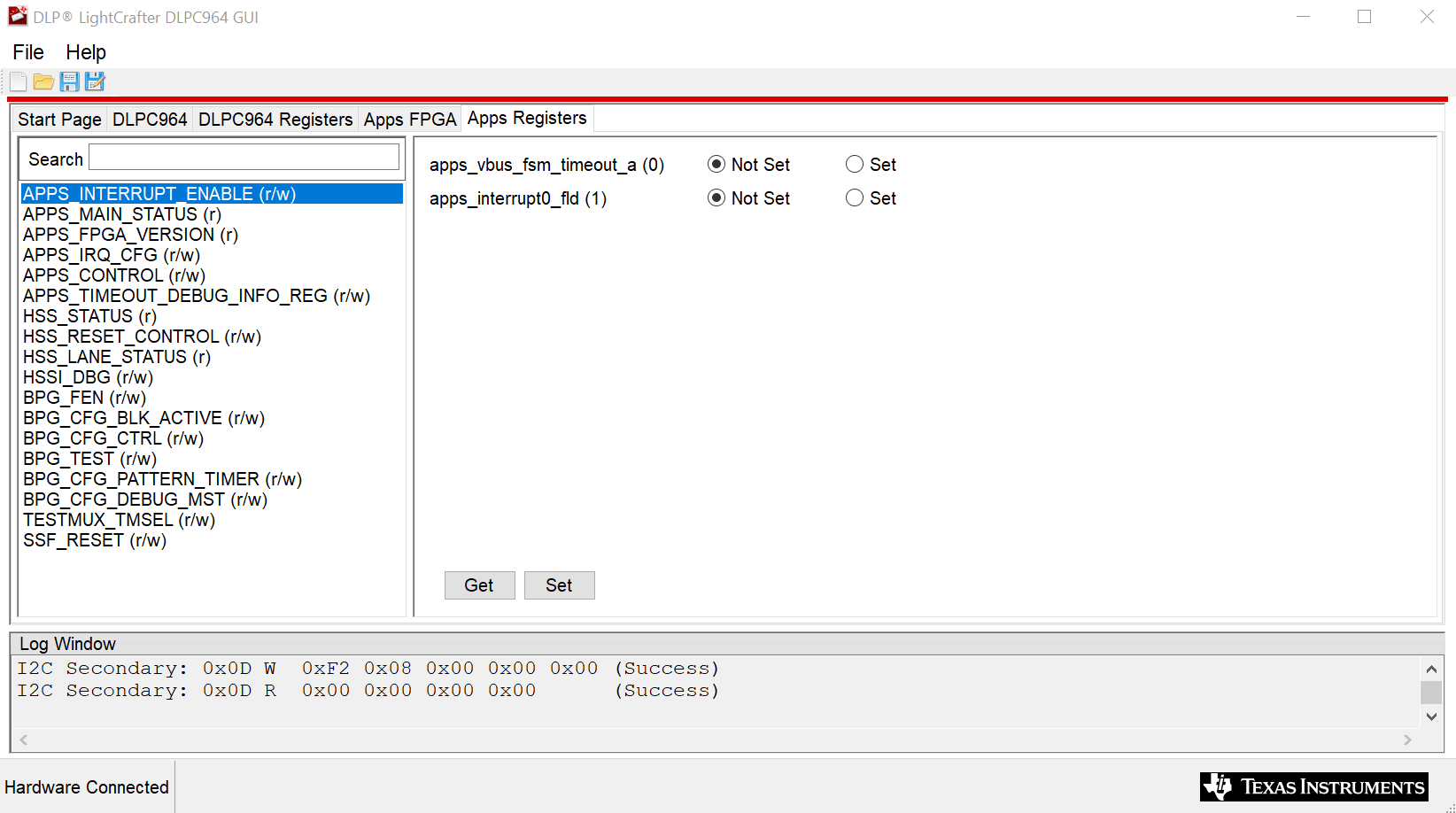
GUID-20240107-SS0I-MFJH-NQH2-VQDGVTM86QP9-low.png Figure 3-18 Apps FPGA Register List

Register Definitions

The following designations are used throughout this section of the document:

  • R - designates read only
  • W - designates write only
  • R/W - designates read and write
  • S - designates status of register
  • I - designates interrupt only
  • P - designates pulse only

Please visit the DLPC964 data sheet for detailed descriptions of each Apps FPGA register offered in the DLPC964 GUI.