JAJS124Q December 1999 – October 2019 UCC1895 , UCC2895 , UCC3895
PRODUCTION DATA.
- 1 特長
- 2 アプリケーション
- 3 概要
- 4 改訂履歴
- 5 Pin Configuration and Functions
- 6 Specifications
-
7 Detailed Description
- 7.1 Overview
- 7.2 Functional Block Diagrams
- 7.3
Feature Description
- 7.3.1 ADS (Adaptive Delay Set)
- 7.3.2 CS (Current Sense)
- 7.3.3 CT (Oscillator Timing Capacitor)
- 7.3.4 DELAB and DELCD (Delay Programming Between Complementary Outputs)
- 7.3.5 EAOUT, EAP, and EAN (Error Amplifier)
- 7.3.6 OUTA, OUTB, OUTC, and OUTD (Output MOSFET Drivers)
- 7.3.7 PGND (Power Ground)
- 7.3.8 RAMP (Inverting Input of the PWM Comparator)
- 7.3.9 REF (Voltage Reference)
- 7.3.10 RT (Oscillator Timing Resistor)
- 7.3.11 GND (Analog Ground)
- 7.3.12 SS/DISB (Soft Start/Disable)
- 7.3.13 SYNC (Oscillator Synchronization)
- 7.3.14 VDD (Chip Supply)
- 7.4 Device Functional Modes
- 7.5 Programming
-
8 Application and Implementation
- 8.1 Application Information
- 8.2
Typical Application
- 8.2.1 Design Requirements
- 8.2.2
Detailed Design Procedure
- 8.2.2.1 Power Loss Budget
- 8.2.2.2 Preliminary Transformer Calculations (T1)
- 8.2.2.3 QA, QB, QC, QD FET Selection
- 8.2.2.4 Selecting LS
- 8.2.2.5 Selecting Diodes DB and DC
- 8.2.2.6 Output Inductor Selection (LOUT)
- 8.2.2.7 Output Capacitance (COUT)
- 8.2.2.8 Select Rectifier Diodes
- 8.2.2.9 Input Capacitance (CIN)
- 8.2.2.10 Current Sense Network (CT, RCS, RR, DA)
- 8.2.3 Application Curves
- 9 Power Supply Recommendations
- 10Layout
- 11デバイスおよびドキュメントのサポート
- 12メカニカル、パッケージ、および注文情報
7.2 Functional Block Diagrams
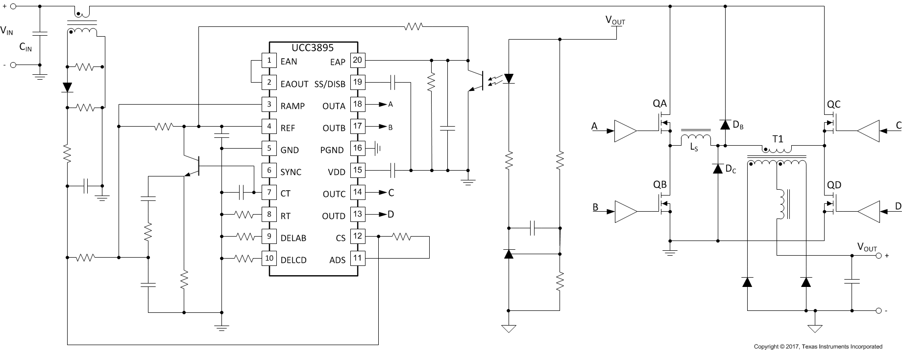 Figure 9. Simplified Application Diagram
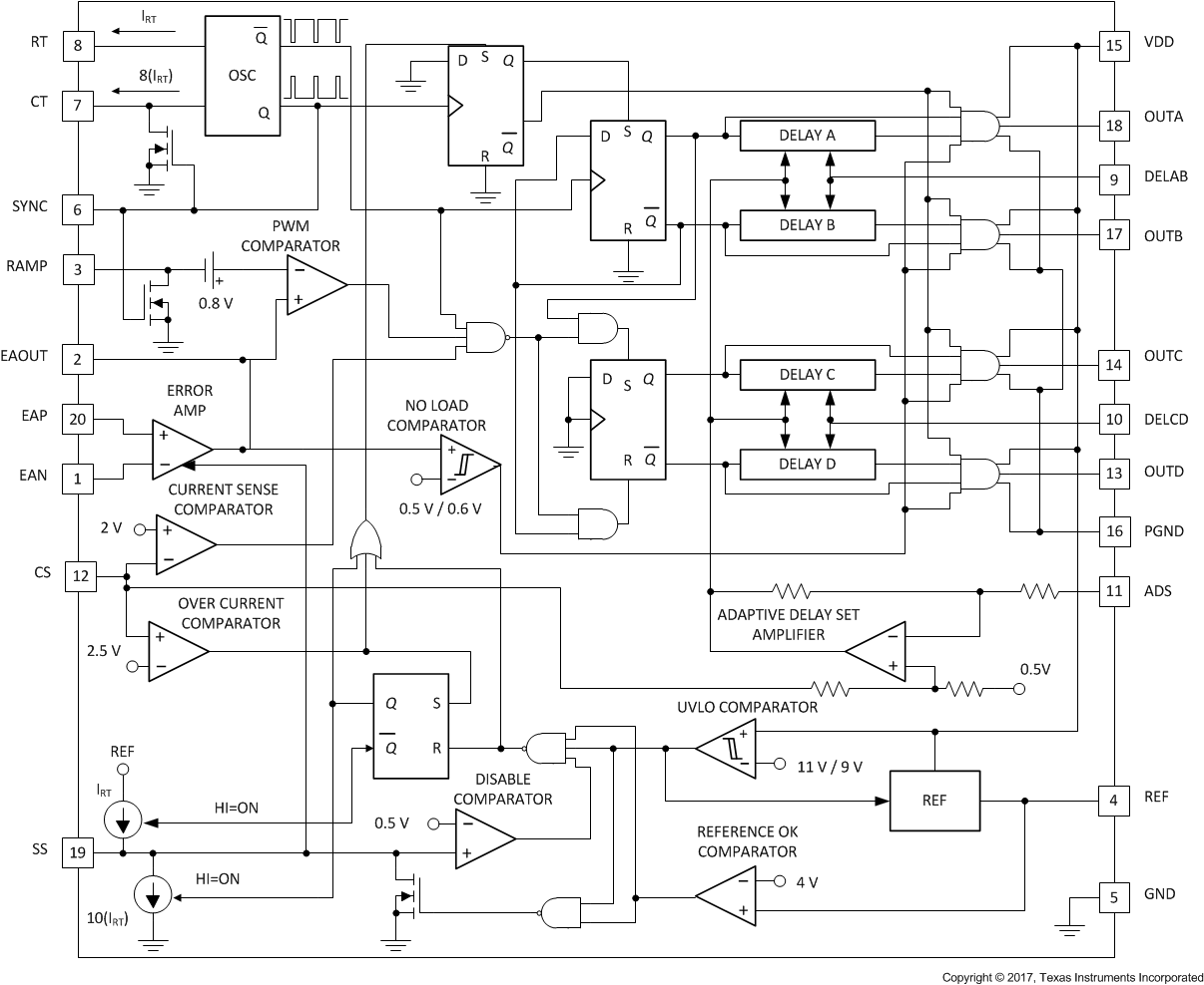
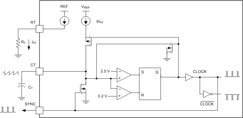 Figure 11. Oscillator Block Diagram
 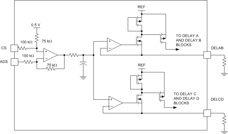 Figure 12. Adaptive Delay Set Block Diagram
 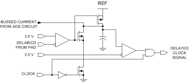 Figure 13. Delay Block Diagram (One Delay Block Per Outlet)