JAJS194E January 2007 – June 2019 TPS40077
PRODUCTION DATA.
- 1 特長
- 2 アプリケーション
- 3 概要
- 4 改訂履歴
- 5 Pin Configuration and Functions
- 6 Specifications
-
7 Detailed Description
- 7.1 Overview
- 7.2 Functional Block Diagram
- 7.3
Feature Description
- 7.3.1 Minimum Pulse Duration
- 7.3.2 Slew Rate Limit On VDD
- 7.3.3 Setting The Switching Frequency (Programming The Clock Oscillator)
- 7.3.4 Loop Compensation
- 7.3.5 Shutdown and Sequencing
- 7.3.6 Boost and LVBP Bypass Capacitance
- 7.3.7 Internal Regulators
- 7.3.8 Power Dissipation
- 7.3.9 Boost Diode
- 7.3.10 Synchronous Rectifier Control
- 7.4 Programming
-
8 Application and Implementation
- 8.1 Application Information
- 8.2
Typical Applications
- 8.2.1
Buck Regulator 8-V to 16-V Input, 1.8-V Output at 10 A
- 8.2.1.1 Design Requirements
- 8.2.1.2
Detailed Design Procedure
- 8.2.1.2.1
Power Train Components
- 8.2.1.2.1.1 Output Inductor, LOUT
- 8.2.1.2.1.2 Output Capacitor, COUT, ELCO and MLCC
- 8.2.1.2.1.3 Input Capacitor, CIN ELCO and MLCC
- 8.2.1.2.1.4 Switching MOSFET, QSW
- 8.2.1.2.1.5 Rectifier MOSFET, QSR
- 8.2.1.2.1.6 Timing Resistor, RT
- 8.2.1.2.1.7 Feed-Forward and UVLO Resistor, RKFF
- 8.2.1.2.1.8 Soft-Start Capacitor, CSS
- 8.2.1.2.1.9 Short-Circuit Protection, RILIM and CILIM
- 8.2.1.2.1.10 Boost Voltage, CBOOST and DBOOST (Optional)
- 8.2.1.2.1.11 Closing the Feedback Loop, RZ1, RP1, RPZ2, RSET1, RSET2, CZ2, CP2, and CPZ1
- 8.2.1.2.1
Power Train Components
- 8.2.1.3 Application Curves
- 8.2.1
Buck Regulator 8-V to 16-V Input, 1.8-V Output at 10 A
- 8.3 Additional System Examples
- 9 Layout
- 10デバイスおよびドキュメントのサポート
- 11メカニカル、パッケージ、および注文情報
6.5 Typical Characteristics
 Figure 1. LVBP Voltage vs Junction Temperature
  Figure 3. DBP Voltage vs Junction Temperature
  Figure 5. Current Limit Offset Voltage
vs Junction Temperature
 Figure 7. Feedback Regulation Voltage
vs Junction Temperature
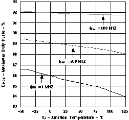 Figure 9. Maximum Duty Cycle
vs Junction Temperature
 Figure 11. Programmable UVLO Threshold
vs Junction Temperature
 Figure 13. Error Amplifier Input Bias Current
vs Junction Temperature
 Figure 15. Switching Frequency
vs Timing Resistance
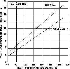 Figure 17. Undervoltage Lockout Threshold
vs Feed-Forward Impedance
 Figure 19. Typical Maximum Duty Cycle
vs Input Voltage
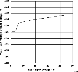 Figure 21. Input Voltage vs Low-Voltage Bypass Voltage
 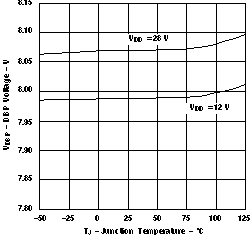 Figure 2. DBP Voltage vs Junction Temperature
 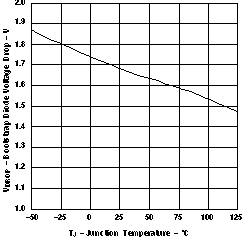 Figure 4. Bootstrap Diode Voltage
vs Junction Temperature
 Figure 6. Current Limit Sink Current
vs Junction Temperature
 Figure 8. Switching Frequency vs Input Voltage
  Figure 10. Undervoltage Lockout
vs Junction Temperature
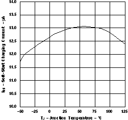 Figure 12. Soft-Start Charging Current
vs Junction Temperature
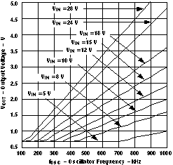 Figure 14. Minimum Output Voltage vs Frequency
 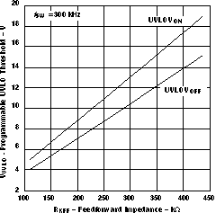 Figure 16. Undervoltage Lockout Threshold
vs Feed-Forward Impedance
 Figure 18. Undervoltage Lockout Threshold
vs Feed-Forward Impedance
 Figure 20. DBP Voltage vs Input Voltage