At TJ = 25°C, VOUT = 1.5V, VIN = VOUT(nom) + 0.3V, VBIAS = 3.3V, IOUT = 50mA, CIN = 1μF, CBIAS = 1μF, CSS = 0.01μF, and COUT = 10μF for legacy chip and TJ = 25°C, VIN = VOUT(nom) + 0.3V, VBIAS = 5V, IOUT = 50mA, VEN = VIN, CIN = 1μF, CBIAS = 4.7μF, and COUT = 10μF for new chip, unless otherwise noted
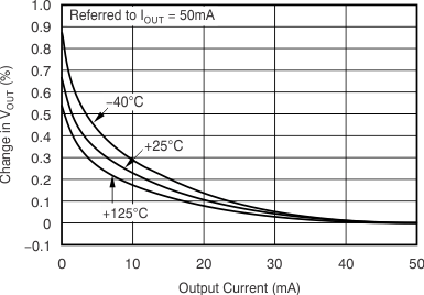
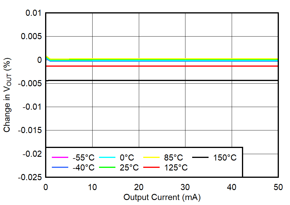
 Figure 5-1 Load Regulation
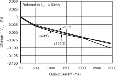
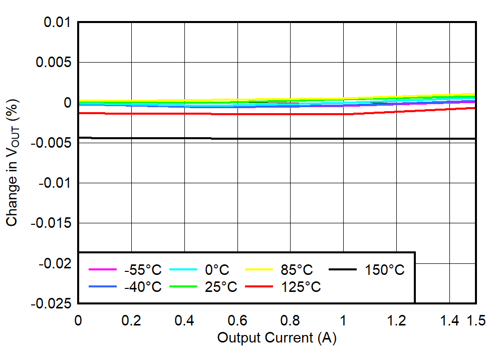
 Figure 5-3 Load Regulation
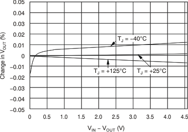
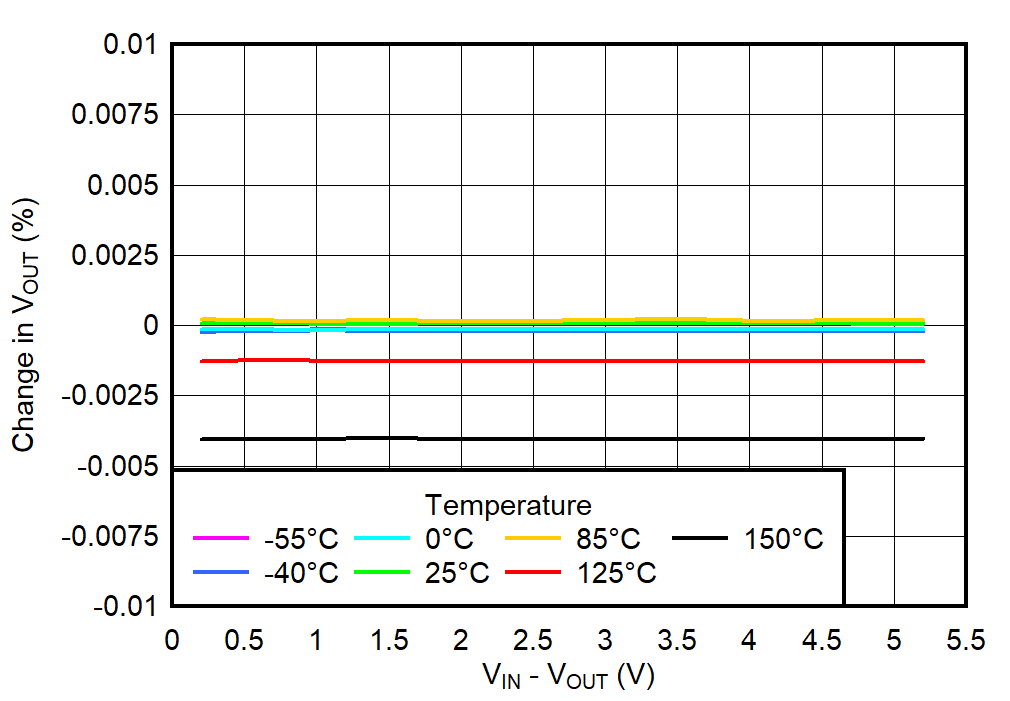
 Figure 5-5 Line Regulation
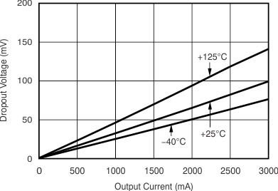
 Figure 5-7 VIN Dropout Voltage vs IOUT and Temperature (TJ)
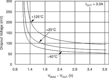
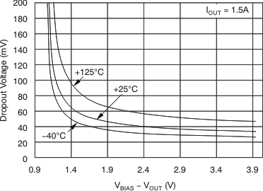
 Figure 5-9 VIN Dropout Voltage vs VBIAS – VOUT and Temperature (TJ)
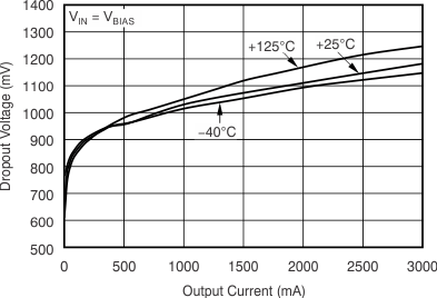
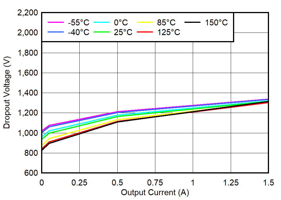
 Figure 5-11 VBIAS Dropout Voltage vs IOUT and Temperature (TJ)
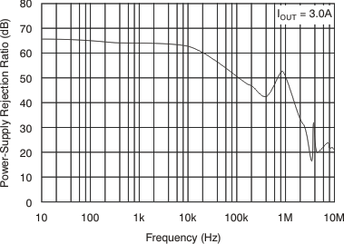
 Figure 5-13 VBIAS PSRR vs Frequency
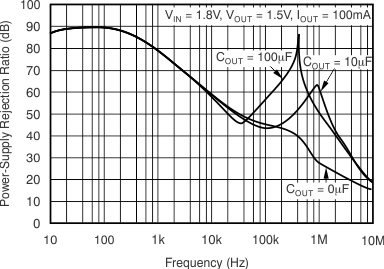
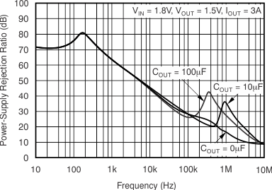
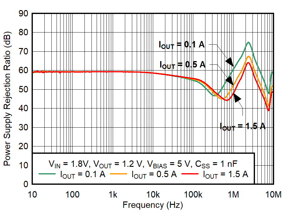
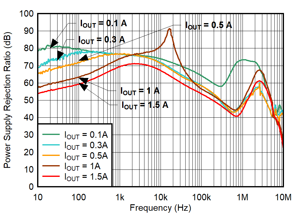
 Figure 5-15 VIN PSRR vs Frequency
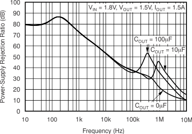
 Figure 5-17 VIN PSRR vs Frequency
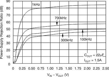
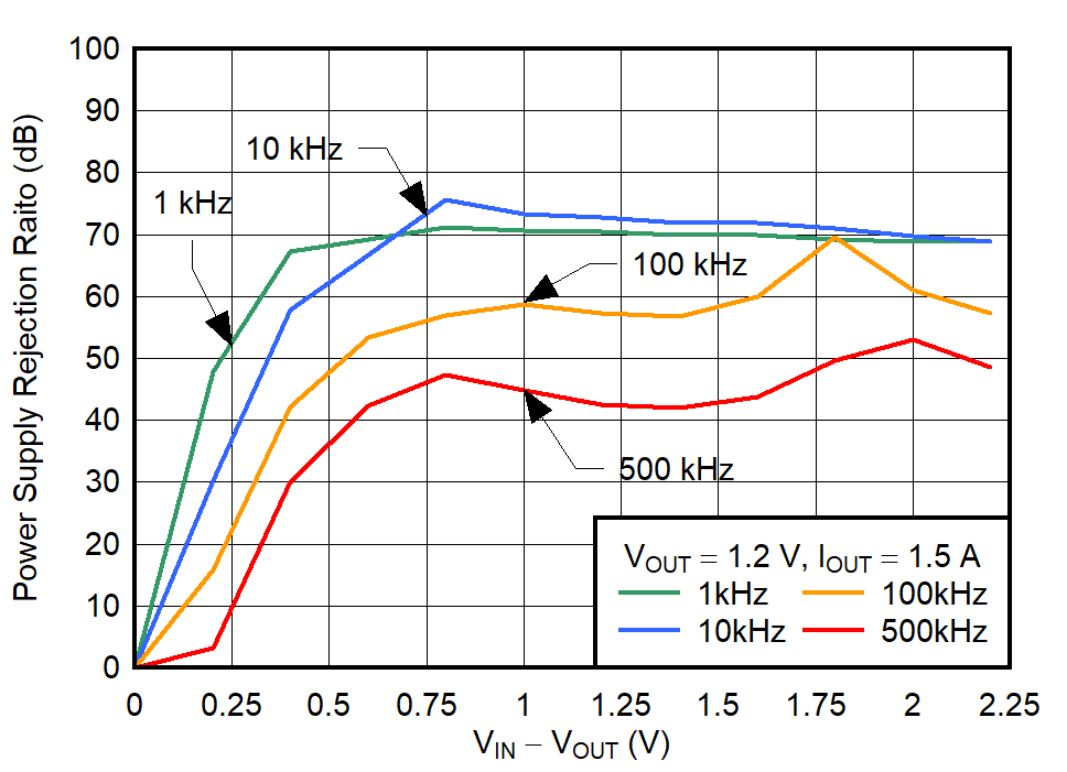
 Figure 5-19 VIN PSRR vs VIN – VOUT
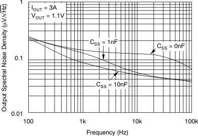
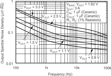
 Figure 5-21 Noise Spectral Density
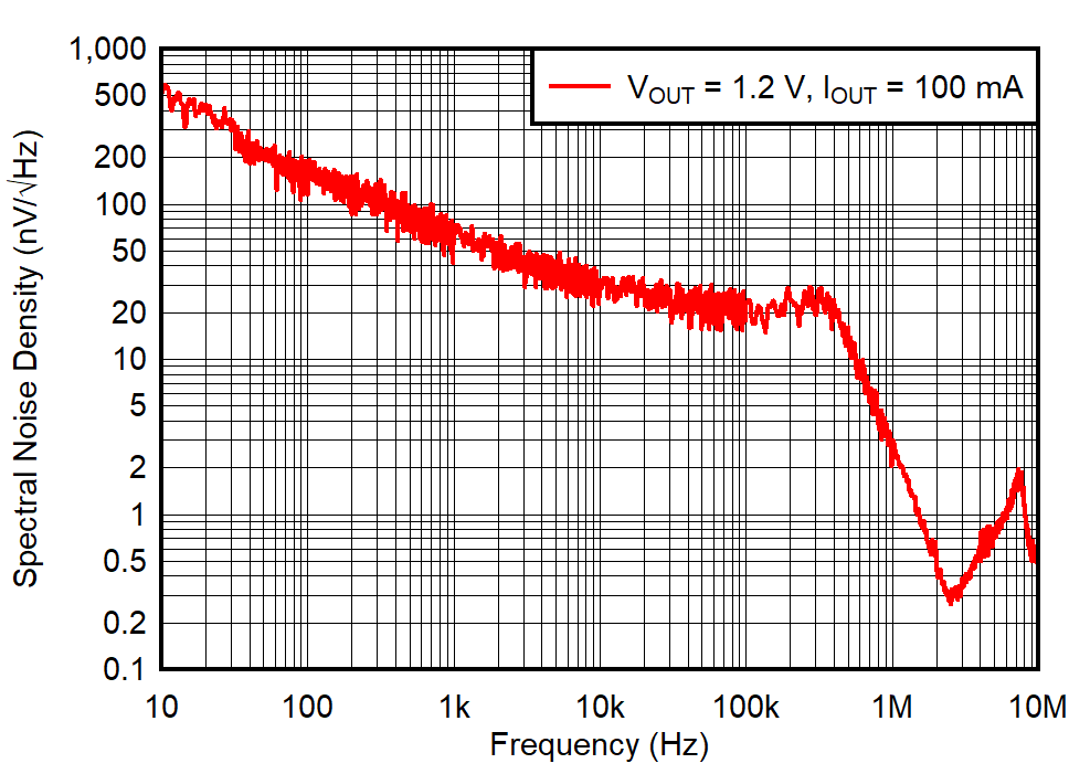
 Figure 5-23 Noise Spectral Density
| New chip, VIN = 1.1V, VOUT = 0.8V |
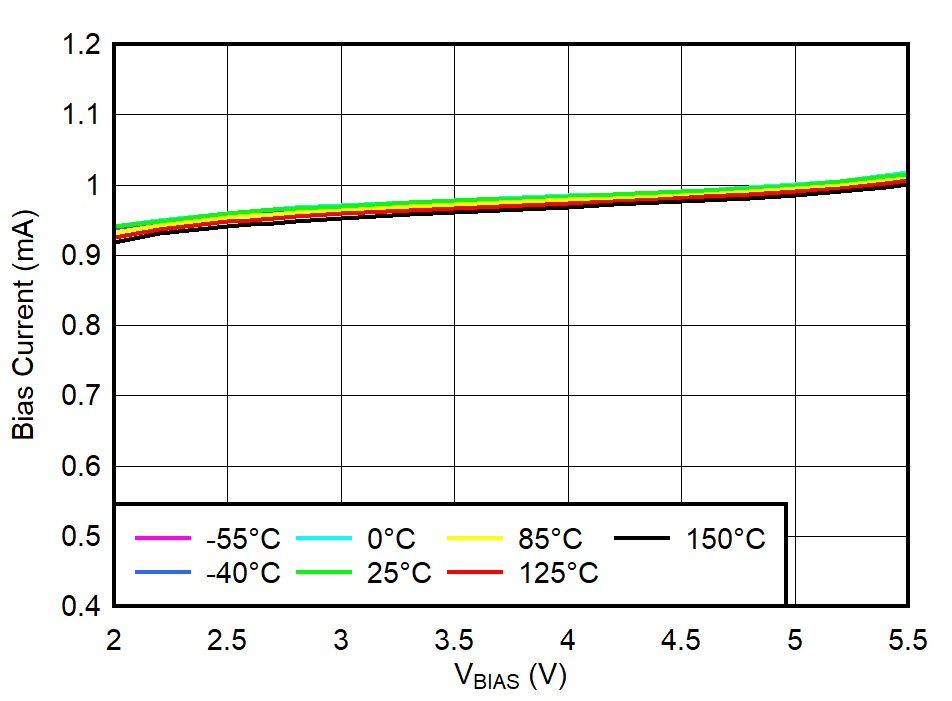
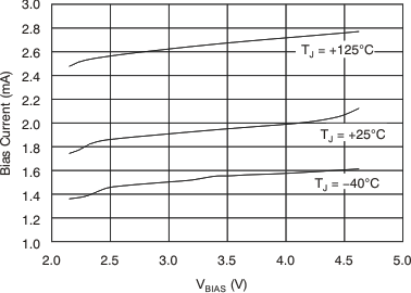
 Figure 5-27 BIAS Pin Current vs
VBIAS and Temperature (TJ)
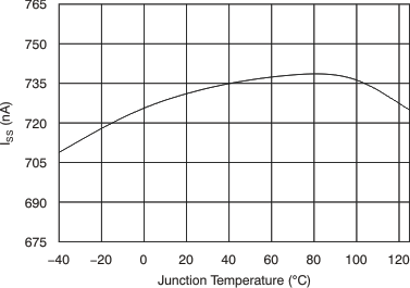
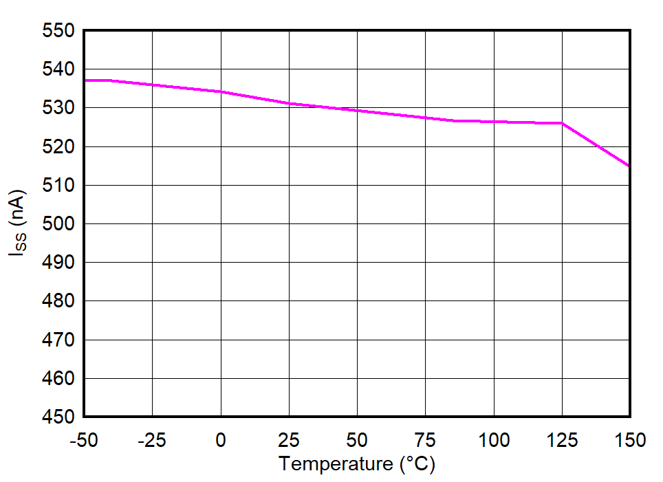
 Figure 5-29 Soft-Start Charging
Current (ISS) vs Temperature
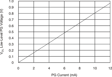
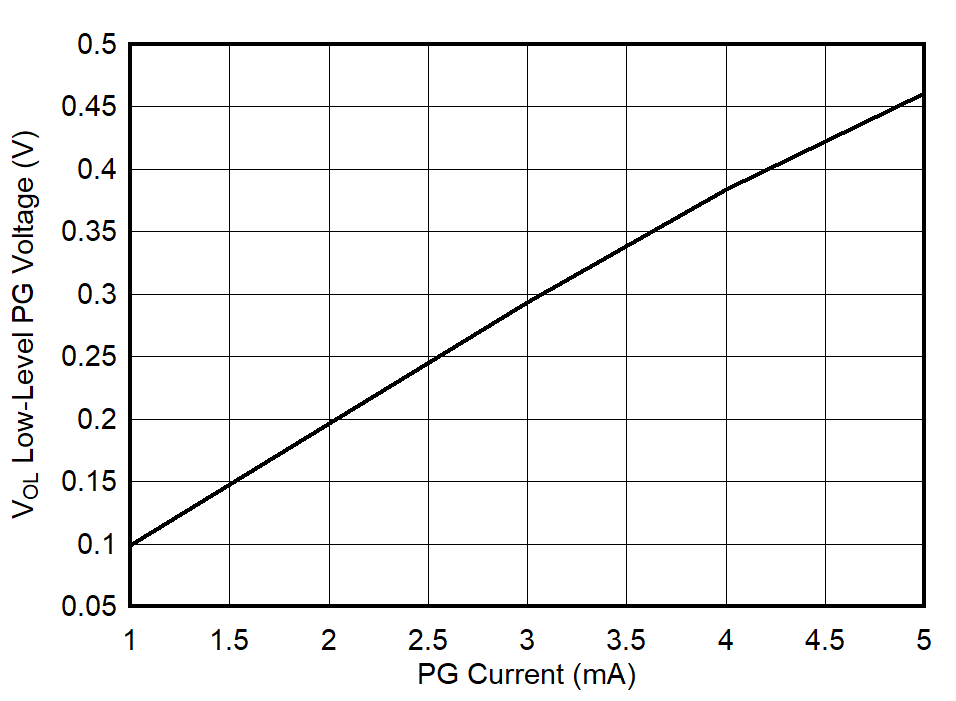
 Figure 5-31 Low-Level PG Voltage vs
PG Current
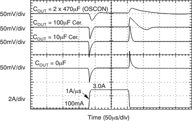
 Figure 5-33 Load Transient Response
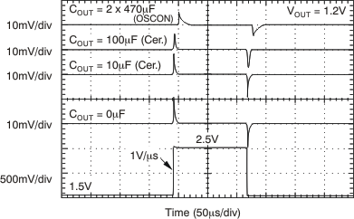
 Figure 5-35 VBIAS Line
Transient (3A)
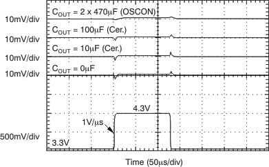
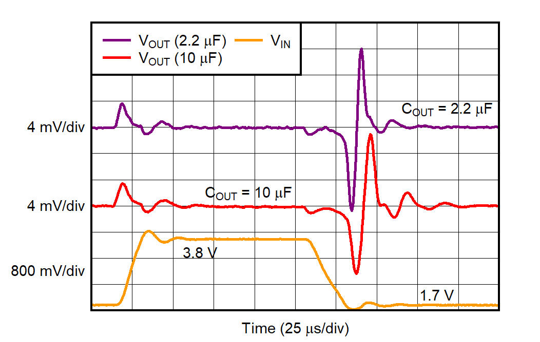
 Figure 5-37 VIN Line
Transient (3A)
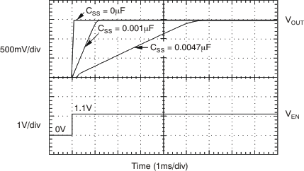
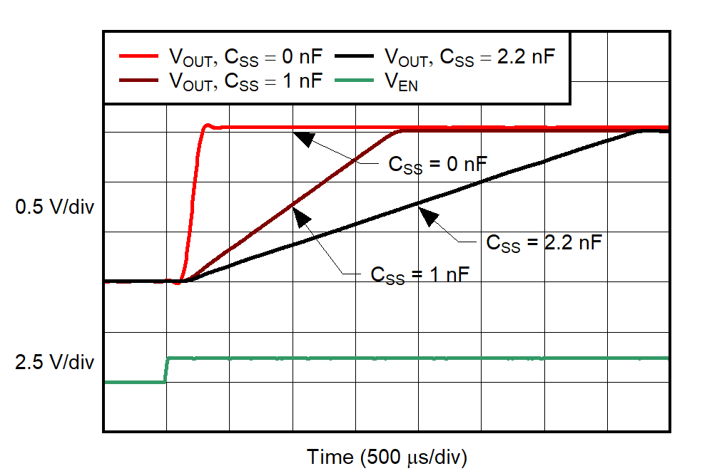
 Figure 5-39 Turn-On Response
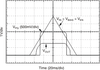
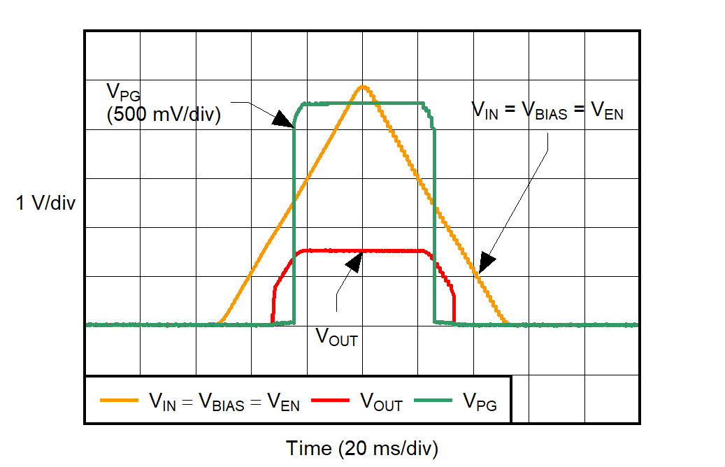
 Figure 5-41 Power-Up, Power-Down
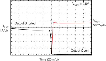
 Figure 5-43 Output Short-Circuit Recovery
 Figure 5-2 Load Regulation at Light Load
 Figure 5-4 Load Regulation
 Figure 5-6 VIN Line Regulation
 Figure 5-8 VIN Dropout Voltage vs IOUT and Temperature (TJ)
 Figure 5-10 VIN Dropout Voltage vs VBIAS – VOUT and Temperature (TJ)
 Figure 5-12 VBIAS Dropout Voltage vs IOUT and Temperature (TJ)
 Figure 5-14 VBIAS PSRR vs Frequency
 Figure 5-16 VIN PSRR vs Frequency
 Figure 5-18 VIN PSRR vs Frequency
 Figure 5-20 VIN PSRR vs (VIN – VOUT)
 Figure 5-22 Noise Spectral Density
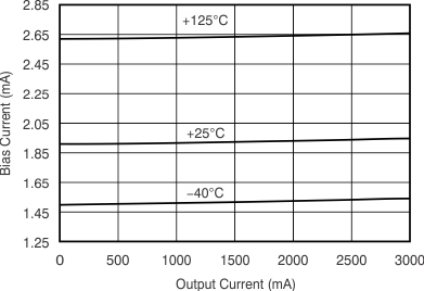
 Figure 5-24 IBIAS vs
Output Current and Temperature
 Figure 5-26 IBIAS vs
VBIAS and VOUT
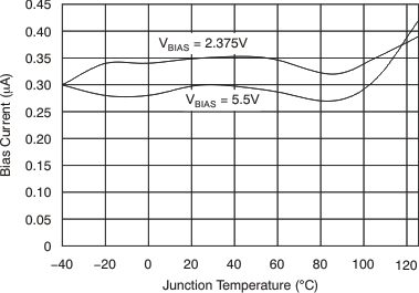
 Figure 5-28 IBIAS Shutdown
vs Temperature
 Figure 5-30 Soft-Start Charging
Current (ISS) vs Temperature (TJ)
 Figure 5-32 Low-Level PG Voltage vs
Current
 Figure 5-34 Load Transient Response
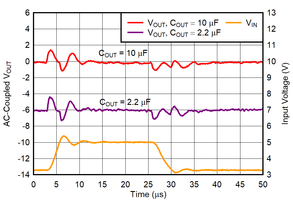
 Figure 5-36 VBIAS Line Transient
 Figure 5-38 VIN Line Transient
 Figure 5-40 Turn-On Response
 Figure 5-42 Power-Up, Power-Down