JAJS204S December   2005  – November 2024 TPS74401

PRODUCTION DATA  

  1.   1
  2. 特長
  3. アプリケーション
  4. 概要
  5. Pin Configuration and Functions
  6. Specifications
    1. 5.1 Absolute Maximum Ratings
    2. 5.2 ESD Ratings
    3. 5.3 Recommended Operating Conditions
    4. 5.4 Thermal Information
    5. 5.5 Electrical Characteristics
    6. 5.6 Typical Characteristics
  7. Detailed Description
    1. 6.1 Overview
    2. 6.2 Functional Block Diagram
    3. 6.3 Feature Description
      1. 6.3.1 Enable, Shutdown
      2. 6.3.2 Power-Good (VQFN Package Only)
      3. 6.3.3 Internal Current Limit
      4. 6.3.4 Thermal Protection
    4. 6.4 Device Functional Modes
      1. 6.4.1 Normal Operation
      2. 6.4.2 Dropout Operation
      3. 6.4.3 Disabled
    5. 6.5 Programming
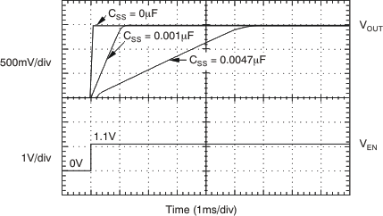
      1. 6.5.1 Programmable Soft-Start
      2. 6.5.2 Sequencing Requirements
  8. Application and Implementation
    1. 7.1 Application Information
      1. 7.1.1 Input, Output, and Bias Capacitor Requirements
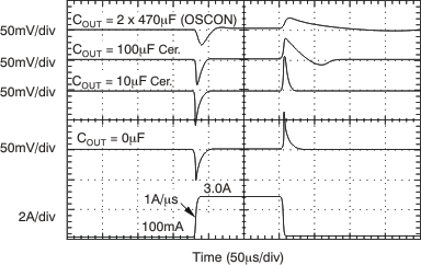
      2. 7.1.2 Transient Response
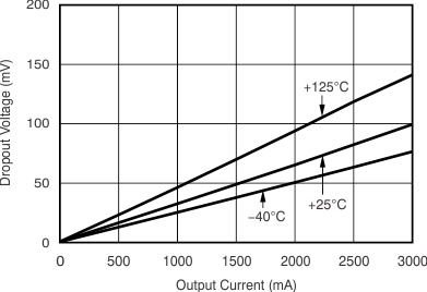
      3. 7.1.3 Dropout Voltage
      4. 7.1.4 Output Noise
    2. 7.2 Typical Applications
      1. 7.2.1 Setting the TPS74401
        1. 7.2.1.1 Design Requirements
        2. 7.2.1.2 Detailed Design Procedure
        3. 7.2.1.3 Application Curves
      2. 7.2.2 Using an Auxiliary Bias Rail
      3. 7.2.3 Without an Auxiliary Bias
    3. 7.3 Power Supply Recommendations
    4. 7.4 Layout
      1. 7.4.1 Layout Guidelines
        1. 7.4.1.1 Power Dissipation
        2. 7.4.1.2 Thermal Considerations
      2. 7.4.2 Layout Example
  9. Device and Documentation Support
    1. 8.1 Documentation Support
      1. 8.1.1 Related Documentation
      2. 8.1.2 Device Nomenclature
    2. 8.2 Device Support
      1. 8.2.1 Development Support
        1. 8.2.1.1 Evaluation Modules
        2. 8.2.1.2 Spice Models
    3. 8.3 ドキュメントの更新通知を受け取る方法
    4. 8.4 サポート・リソース
    5. 8.5 Trademarks
    6. 8.6 静電気放電に関する注意事項
    7. 8.7 用語集
  10. Revision History
  11. 10Mechanical, Packaging, and Orderable Information

Application Curves

TPS74401 Turn-On ResponseFigure 7-2 Turn-On Response
TPS74401 Load
                        Transient ResponseFigure 7-4 Load Transient Response
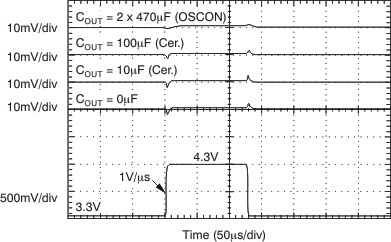
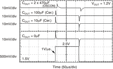
TPS74401 VBIAS Line Transient (3A)Figure 7-6 VBIAS Line Transient (3A)
TPS74401 VIN Dropout Voltage vs IOUT and Temperature
                            (TJ)Figure 7-8 VIN Dropout Voltage vs IOUT and Temperature (TJ)
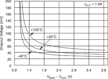
TPS74401 VIN Dropout Voltage vs VBIAS – VOUT
                        and Temperature (TJ)Figure 7-10 VIN Dropout Voltage vs VBIAS – VOUT and Temperature (TJ)
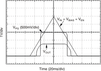
TPS74401 Power-Up, Power-DownFigure 7-3 Power-Up, Power-Down
TPS74401 VIN Line Transient (3A)Figure 7-5 VIN Line Transient (3A)
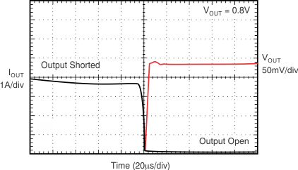
TPS74401 Output Short-Circuit RecoveryFigure 7-7 Output Short-Circuit Recovery
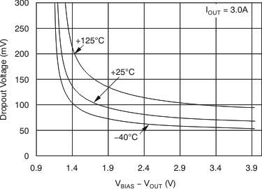
TPS74401 VIN Dropout Voltage vs VBIAS – VOUT
                        and Temperature (TJ)Figure 7-9 VIN Dropout Voltage vs VBIAS – VOUT and Temperature (TJ)
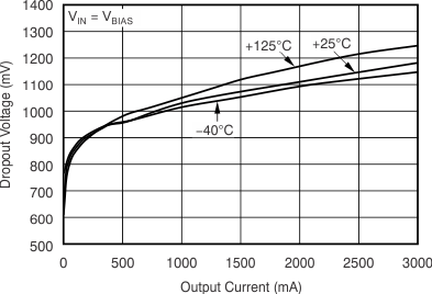
TPS74401 VBIAS Dropout Voltage vs IOUT and Temperature
                            (TJ)Figure 7-11 VBIAS Dropout Voltage vs IOUT and Temperature (TJ)