JAJS249E August   2006  – January 2024 TPS5410

PRODUCTION DATA  

  1.   1
  2. 特長
  3. アプリケーション
  4. 概要
  5. Pin Configuration and Functions
  6. Specifications
    1. 5.1 Absolute Maximum Ratings
    2. 5.2 ESD Ratings
    3. 5.3 Recommended Operating Conditions
    4. 5.4 Thermal Information 
    5. 5.5 Electrical Characteristics
    6. 5.6 Typical Characteristics
  7. Detailed Description
    1. 6.1 Overview
    2. 6.2 Functional Block Diagram
    3. 6.3 Feature Description
      1. 6.3.1  Oscillator Frequency
      2. 6.3.2  Voltage Reference
      3. 6.3.3  Enable (ENA) and Internal Slow-Start
      4. 6.3.4  Undervoltage Lockout (UVLO)
      5. 6.3.5  Boost Capacitor (BOOT)
      6. 6.3.6  Output Feedback (VSENSE)
      7. 6.3.7  Internal Compensation
      8. 6.3.8  Voltage Feed-Forward
      9. 6.3.9  Pulse-Width-Modulation (PWM) Control
      10. 6.3.10 Overcurrent Limiting
      11. 6.3.11 Overvoltage Protection
      12. 6.3.12 Thermal Shutdown
    4. 6.4 Device Functional Modes
      1. 6.4.1 Minimum Input Voltage
      2. 6.4.2 ENA Control
  8. Applications and Implementation
    1. 7.1 Application Information
    2. 7.2 Typical Applications
      1. 7.2.1 Application Circuit
        1. 7.2.1.1 Design Requirements
        2. 7.2.1.2 Detailed Design Procedure
          1. 7.2.1.2.1 Switching Frequency
          2. 7.2.1.2.2 Input Capacitors
          3. 7.2.1.2.3 Output Filter Components
            1. 7.2.1.2.3.1 Inductor Selection
            2. 7.2.1.2.3.2 Capacitor Selection
          4. 7.2.1.2.4 Output Voltage Setpoint
          5. 7.2.1.2.5 Boot Capacitor
          6. 7.2.1.2.6 Catch Diode
          7. 7.2.1.2.7 Advanced Information
            1. 7.2.1.2.7.1 Output Voltage Limitations
            2. 7.2.1.2.7.2 Internal Compensation Network
            3. 7.2.1.2.7.3 Thermal Calculations
        3. 7.2.1.3 Application Curves
      2. 7.2.2 Using All Ceramic Capacitors
        1. 7.2.2.1 Design Requirements
        2. 7.2.2.2 Detailed Design Procedure
          1. 7.2.2.2.1 Output Filter Capacitor Selection
          2. 7.2.2.2.2 External Compensation Network
        3. 7.2.2.3 Application Curves
    3. 7.3 Power Supply Recommendations
    4. 7.4 Layout
      1. 7.4.1 Layout Guidelines
      2. 7.4.2 Layout Example
  9. Device and Documentation Support
    1. 8.1 Documentation Support
      1. 8.1.1 Related Documentation
    2. 8.2 ドキュメントの更新通知を受け取る方法
    3. 8.3 サポート・リソース
    4. 8.4 Trademarks
    5. 8.5 静電気放電に関する注意事項
    6. 8.6 用語集
  10. Revision History
  11. 10Mechanical, Packaging, and Orderable Information
Output Voltage Setpoint

The output voltage of the TPS5410 is set by a resistor divider (R1 and R2) from the output to the VSENSE pin. Calculate the R2 resistor value for the output voltage of 12 V using Equation 12:

Equation 12. GUID-4542A03B-4B5E-49DB-BFF5-373134B0925D-low.gif

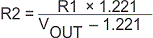
For any TPS5410 design, start with an R1 value of 10 kΩ. R2 is then 1.13 kΩ.