JAJS499J June   2010  – January 2018 TPS7A80

PRODUCTION DATA.  

  1. 特長
  2. アプリケーション
  3. 概要
    1.     Device Images
      1.      標準アプリケーション回路
  4. 改訂履歴
  5. Pin Configuration and Functions
    1.     Pin Functions
  6. Specifications
    1. 6.1 Absolute Maximum Ratings
    2. 6.2 ESD Ratings
    3. 6.3 Recommended Operating Conditions
    4. 6.4 Thermal Information
    5. 6.5 Electrical Characteristics
    6. 6.6 Typical Characteristics
  7. Detailed Description
    1. 7.1 Overview
    2. 7.2 Functional Block Diagram
    3. 7.3 Feature Description
      1. 7.3.1 Internal Current Limit
      2. 7.3.2 Shutdown
      3. 7.3.3 Start-Up
      4. 7.3.4 Undervoltage Lockout (UVLO)
    4. 7.4 Device Functional Modes
  8. Application and Implementation
    1. 8.1 Application Information
    2. 8.2 Typical Application
      1. 8.2.1 Design Requirements
        1. 8.2.1.1 Dropout Voltage
        2. 8.2.1.2 Minimum Load
        3. 8.2.1.3 Input and Output Capacitor Requirements
        4. 8.2.1.4 Transient Response
      2. 8.2.2 Detailed Design Procedure
        1. 8.2.2.1 Output Noise
      3. 8.2.3 Application Curve
  9. Power Supply Recommendations
  10. 10Layout
    1. 10.1 Layout Guidelines
      1. 10.1.1 Board Layout Recommendations to Improve PSRR and Noise Performance
      2. 10.1.2 Thermal Considerations
      3. 10.1.3 Power Dissipation
      4. 10.1.4 Estimating Junction Temperature
    2. 10.2 Layout Example
  11. 11デバイスおよびドキュメントのサポート
    1. 11.1 ドキュメントのサポート
      1. 11.1.1 関連資料
    2. 11.2 ドキュメントの更新通知を受け取る方法
    3. 11.3 コミュニティ・リソース
    4. 11.4 商標
    5. 11.5 静電気放電に関する注意事項
    6. 11.6 Glossary
  12. 12メカニカル、パッケージ、および注文情報

Estimating Junction Temperature

Using the thermal metrics ΨJT and ΨJB, as shown in the Thermal Information table, the junction temperature can be estimated with corresponding formulas (given in Equation 6). For backwards compatibility, an older θJC,Top parameter is listed as well.

Equation 6. TPS7A80 q_new_metrics_bvs066.gif

Where PD is the power dissipation shown by Equation 5, TT is the temperature at the center-top of the IC package, and TB is the PCB temperature measured 1 mm away from the IC package on the PCB surface (as Figure 36 shows).

NOTE

Both TT and TB can be measured on actual application boards using a thermo gun (an infrared thermometer).

For more information about measuring TT and TB, see Using New Thermal Metrics.

By looking at Figure 35, the new thermal metrics (ΨJT and ΨJB) have very little dependency onboard size. That is, using ΨJT or ΨJB with Equation 6 is a good way to estimate TJ by simply measuring TT or TB, regardless of the application board size.
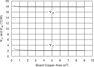
TPS7A80 ai_psi_jt_jb_bvs135.gifFigure 35. ΨJT and ΨJB vs Board Size

For a more detailed discussion of why TI does not recommend using θJC(top) to determine thermal characteristics, see Using New Thermal Metrics. For further information, see Semiconductor and IC Package Thermal Metrics.
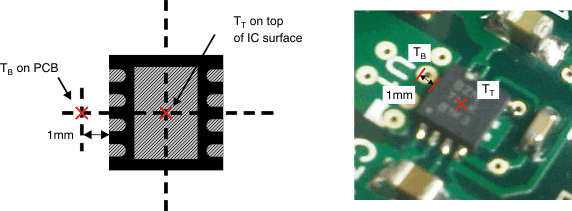
TPS7A80 ai_measuring_point_bvs135.gifFigure 36. Measuring Points for TT and TB