JAJS503C June   2008  – July 2018 ADS7950 , ADS7951 , ADS7952 , ADS7953 , ADS7954 , ADS7955 , ADS7956 , ADS7957 , ADS7958 , ADS7959 , ADS7960 , ADS7961

PRODUCTION DATA.  

  1. 特長
  2. アプリケーション
    1.     詳細ブロック図
  3. 概要
  4. 改訂履歴
  5. デバイス比較表
  6. Pin Configuration and Functions
    1.     Pin Functions: TSSOP Packages
    2.     Pin Functions: VQFN Packages
  7. Specifications
    1. 7.1  Absolute Maximum Ratings
    2. 7.2  ESD Ratings
    3. 7.3  Recommended Operating Conditions
    4. 7.4  Thermal Information: TSSOP
    5. 7.5  Thermal Information: VQFN
    6. 7.6  Electrical Characteristics: ADS7950, ADS7951, ADS7952, ADS7953
    7. 7.7  Electrical Characteristics, ADS7954, ADS7955, ADS7956, ADS7957
    8. 7.8  Electrical Characteristics, ADS7958, ADS7959, ADS7960, ADS7961
    9. 7.9  Timing Requirements
    10. 7.10 Typical Characteristics (All ADS79xx Family Devices)
    11. 7.11 Typical Characteristics (12-Bit Devices Only)
    12. 7.12 Typical Characteristics (12-Bit Devices Only)
  8. Detailed Description
    1. 8.1 Overview
    2. 8.2 Functional Block Diagram
    3. 8.3 Feature Description
      1. 8.3.1 Reference
      2. 8.3.2 Power Saving
    4. 8.4 Device Functional Modes
      1. 8.4.1 Channel Sequencing Modes
      2. 8.4.2 Device Programming and Mode Control
        1. 8.4.2.1 Mode Control Register
        2. 8.4.2.2 Program Registers
      3. 8.4.3 Device Power-Up Sequence
      4. 8.4.4 Operating in Manual Mode
      5. 8.4.5 Operating in Auto-1 Mode
      6. 8.4.6 Operating in Auto-2 Mode
      7. 8.4.7 Continued Operation in a Selected Mode
    5. 8.5 Programming
      1. 8.5.1 Digital Output
      2. 8.5.2 GPIO Registers
      3. 8.5.3 Alarm Thresholds for GPIO Pins
  9. Application and Implementation
    1. 9.1 Application Information
      1. 9.1.1 Analog Input
    2. 9.2 Typical Applications
      1. 9.2.1 Unbuffered Multiplexer Output (MXO)
        1. 9.2.1.1 Design Requirements
        2. 9.2.1.2 Detailed Design Procedure
        3. 9.2.1.3 Application Curves
      2. 9.2.2 OPA192 Buffered Multiplexer Output (MXO)
        1. 9.2.2.1 Design Requirements
        2. 9.2.2.2 Detailed Design Procedure
        3. 9.2.2.3 Application Curves
  10. 10Power Supply Recommendations
  11. 11Layout
    1. 11.1 Layout Guidelines
    2. 11.2 Layout Examples
  12. 12デバイスおよびドキュメントのサポート
    1. 12.1 ドキュメントのサポート
      1. 12.1.1 関連資料
    2. 12.2 関連リンク
    3. 12.3 ドキュメントの更新通知を受け取る方法
    4. 12.4 コミュニティ・リソース
    5. 12.5 商標
    6. 12.6 静電気放電に関する注意事項
    7. 12.7 Glossary
  13. 13メカニカル、パッケージ、および注文情報

Timing Requirements

All specifications typical at –40°C to 125°C, +VA = 2.7 V to 5.25 V (unless otherwise specified)(1)(2) (see Figure 1, Figure 2, Figure 3, and Figure 4)
MIN NOM MAX UNIT
tconv Conversion time +VBD = 1.8 V 16 SCLK
+VBD = 3 V 16
+VBD = 5 V 16
tq Minimum quiet sampling time needed from bus 3-state to start of next conversion +VBD = 1.8 V 40 ns
+VBD = 3 V 40
+VBD = 5 V 40
td1 Delay time, CS low to first data (DO–15) out +VBD = 1.8 V 38 ns
+VBD = 3 V 27
+VBD = 5 V 17
tsu1 Setup time, CS low to first rising edge of SCLK +VBD = 1.8 V 8 ns
+VBD = 3 V 6
+VBD = 5 V 4
td2 Delay time, SCLK falling to SDO next data bit valid +VBD = 1.8 V 35 ns
+VBD = 3 V 27
+VBD = 5 V 17
th1 Hold time, SCLK falling to SDO data bit valid +VBD = 1.8 V 7 ns
+VBD = 3 V 5
+VBD = 5 V 3
td3 Delay time, 16th SCLK falling edge to SDO 3-state +VBD = 1.8 V 26 ns
+VBD = 3 V 22
+VBD = 5 V 13
tsu2 Setup time, SDI valid to rising edge of SCLK +VBD = 1.8 V 2 ns
+VBD = 3 V 3
+VBD = 5 V 4
th2 Hold time, rising edge of SCLK to SDI valid +VBD = 1.8 V 12 ns
+VBD = 3 V 10
+VBD = 5 V 6
tw1 Pulse duration CS high +VBD = 1.8 V 20 ns
+VBD = 3 V 20
+VBD = 5 V 20
td4 Delay time CS high to SDO 3-state +VBD = 1.8 V 24 ns
+VBD = 3 V 21
+VBD = 5 V 12
twh Pulse duration SCLK high +VBD = 1.8 V 20 ns
+VBD = 3 V 20
+VBD = 5 V 20
twl Pulse duration SCLK low +VBD = 1.8 V 20 ns
+VBD = 3 V 20
+VBD = 5 V 20
Frequency SCLK +VBD = 1.8 V 20 MHz
+VBD = 3 V 20
+VBD = 5 V 20
1.8V specifications apply from 1.7 V to 1.9 V, 3 V specifications apply from 2.7 V to 3.6 V, 5 V specifications apply from 4.75 V to 5.25 V.
With 50-pF load
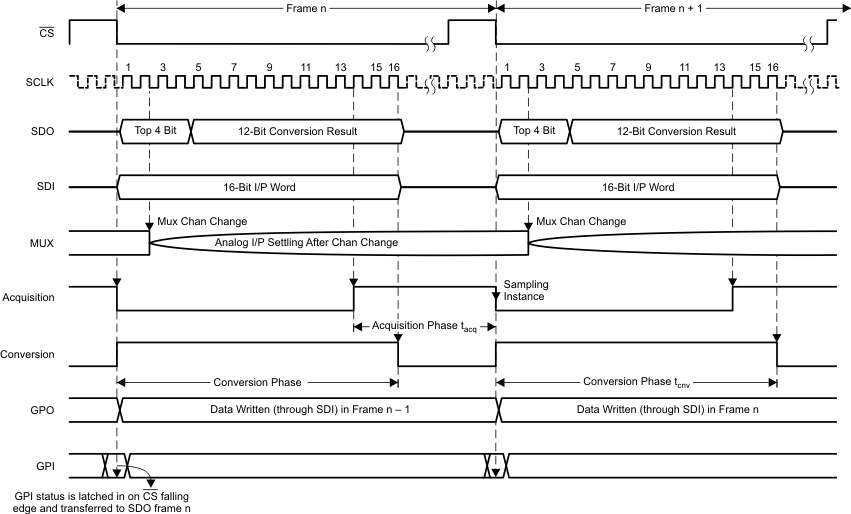
ADS7950 ADS7951 ADS7952 ADS7953 ADS7954 ADS7955 ADS7956 ADS7957 ADS7958 ADS7959 ADS7960 ADS7961 t_dia_las605.gifFigure 1. Device Operation Timing Diagram
ADS7950 ADS7951 ADS7952 ADS7953 ADS7954 ADS7955 ADS7956 ADS7957 ADS7958 ADS7959 ADS7960 ADS7961 t12_dia_las605.gifFigure 2. Serial Interface Timing Diagram for 12-Bit Devices (ADS7950/51/52/53)
ADS7950 ADS7951 ADS7952 ADS7953 ADS7954 ADS7955 ADS7956 ADS7957 ADS7958 ADS7959 ADS7960 ADS7961 tim_10b_las605.gifFigure 3. Serial Interface Timing Diagram for 10-Bit Devices (ADS7954/55/56/57)
ADS7950 ADS7951 ADS7952 ADS7953 ADS7954 ADS7955 ADS7956 ADS7957 ADS7958 ADS7959 ADS7960 ADS7961 tim_8b_las605.gifFigure 4. Serial Interface Timing Diagram for 8-Bit Devices (ADS7958/59/60/61)