JAJS617C
July 1999 – July 2016
DS90LV048A
PRODUCTION DATA.
1
特長
2
アプリケーション
3
概要
4
改訂履歴
5
Pin Configuration and Functions
6
Specifications
6.1
Absolute Maximum Ratings
6.2
ESD Ratings
6.3
Recommended Operating Conditions
6.4
Thermal Information
6.5
Electrical Characteristics
6.6
Switching Characteristics
6.7
Typical Characteristics
7
Parameter Measurement Information
8
Detailed Description
8.1
Overview
8.2
Functional Block Diagram
8.3
Feature Description
8.3.1
Fail-Safe Feature
8.4
Device Functional Modes
9
Application and Implementation
9.1
Application Information
9.2
Typical Application
9.2.1
Design Requirements
9.2.2
Detailed Design Procedure
9.2.2.1
Probing LVDS Transmission Lines
9.2.2.2
Threshold
9.2.3
Application Curve
10
Power Supply Recommendations
11
Layout
11.1
Layout Guidelines
11.1.1
Power Decoupling Recommendations
11.1.2
Differential Traces
11.1.3
Termination
11.2
Layout Example
12
デバイスおよびドキュメントのサポート
12.1
ドキュメントのサポート
12.1.1
関連資料
12.2
ドキュメントの更新通知を受け取る方法
12.3
コミュニティ・リソース
12.4
商標
12.5
静電気放電に関する注意事項
12.6
Glossary
13
メカニカル、パッケージ、および注文情報
7 Parameter Measurement Information
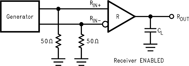
Figure 15. Receiver Propagation Delay and Transition Time Test Circuit
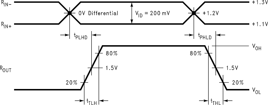
Figure 16. Receiver Propagation Delay and Transition Time Waveforms
C
L
includes load and test jig capacitance.
S
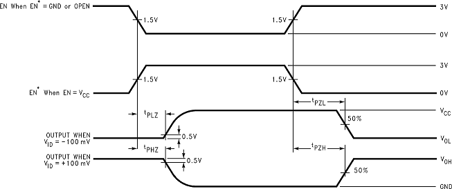
1
= V
CC
for t
PZL
and t
PLZ
measurements.
S
1
= GND for t
PZH
and t
PHZ
measurements.
Figure 17. Receiver TRI-STATE Delay Test Circuit
Figure 18. Receiver TRI-STATE Delay Waveforms