JAJSBH1D July   2011  – October 2016 BQ76925

PRODUCTION DATA.  

  1. 特長
  2. アプリケーション
  3. 概要
  4. 改訂履歴
  5. 概要(続き)
  6. Pin Configuration and Functions
  7. Specifications
    1. 7.1  Absolute Maximum Ratings
    2. 7.2  ESD Ratings
    3. 7.3  Recommended Operating Conditions
    4. 7.4  Thermal Information
    5. 7.5  Electrical Characteristics: Supply Current
    6. 7.6  Internal Power Control (Startup and Shutdown)
    7. 7.7  3.3-V Voltage Regulator
    8. 7.8  Voltage Reference
    9. 7.9  Cell Voltage Amplifier
    10. 7.10 Current Sense Amplifier
    11. 7.11 Overcurrent Comparator
    12. 7.12 Internal Temperature Measurement
    13. 7.13 Cell Balancing and Open Cell Detection
    14. 7.14 I2C Compatible Interface
    15. 7.15 Typical Characteristics
  8. Detailed Description
    1. 8.1 Overview
    2. 8.2 Functional Block Diagram
    3. 8.3 Feature Description
      1. 8.3.1 Internal LDO Voltage Regulator
      2. 8.3.2 ADC Interface
        1. 8.3.2.1 Reference Voltage
          1. 8.3.2.1.1 Host ADC Calibration
        2. 8.3.2.2 Cell Voltage Monitoring
          1. 8.3.2.2.1 Cell Amplifier Headroom Under Extreme Cell Imbalance
          2. 8.3.2.2.2 Cell Amplifier Headroom Under BAT Voltage Drop
        3. 8.3.2.3 Current Monitoring
        4. 8.3.2.4 Overcurrent Monitoring
        5. 8.3.2.5 Temperature Monitoring
          1. 8.3.2.5.1 Internal Temperature Monitoring
      3. 8.3.3 Cell Balancing and Open Cell Detection
    4. 8.4 Device Functional Modes
      1. 8.4.1 Power Modes
        1. 8.4.1.1 POWER ON RESET (POR)
        2. 8.4.1.2 STANDBY
        3. 8.4.1.3 SLEEP
    5. 8.5 Programming
      1. 8.5.1 Host Interface
        1. 8.5.1.1 I2C Addressing
        2. 8.5.1.2 Bus Write Command to bq76925
        3. 8.5.1.3 Bus Read Command from bq76925 Device
    6. 8.6 Register Maps
      1. 8.6.1 Register Descriptions
  9. Application and Implementation
    1. 9.1 Application Information
      1. 9.1.1 Recommended System Implementation
        1. 9.1.1.1 Voltage, Current, and Temperature Outputs
        2. 9.1.1.2 Power Management
        3. 9.1.1.3 Low Dropout (LDO) Regulator
        4. 9.1.1.4 Input Filters
        5. 9.1.1.5 Output Filters
      2. 9.1.2 Cell Balancing
    2. 9.2 Typical Application
      1. 9.2.1 Design Requirements
      2. 9.2.2 Detailed Design Procedure
      3. 9.2.3 Application Curves
  10. 10Power Supply Recommendations
  11. 11Layout
    1. 11.1 Layout Guidelines
    2. 11.2 Layout Example
  12. 12デバイスおよびドキュメントのサポート
    1. 12.1 ドキュメントのサポート
      1. 12.1.1 関連資料
    2. 12.2 ドキュメントの更新通知を受け取る方法
    3. 12.3 コミュニティ・リソース
    4. 12.4 商標
    5. 12.5 静電気放電に関する注意事項
    6. 12.6 Glossary
  13. 13メカニカル、パッケージ、および注文情報

Layout

Layout Guidelines

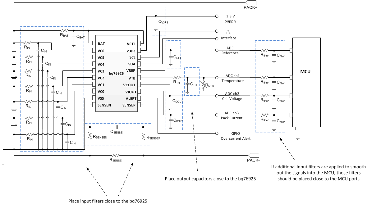
  1. Place input filters for BAT, VCx, and SENSEN/P close to the device
  2. Place output capacitors on V3P3, VREF, VCOUT, and VIOUT close to the device
  3. Please output filters (if any) close to the target device (for example, the MCU ADC input ports)
  4. Isolate high-current and low-current groundings. The AFE, filter capacitors, and MCU grounds should connect to the low-current ground plane of the PCB.

Layout Example

bq76925 layout_filter_place_lusam9.gif Figure 21. Filters and Bypass Capacitors Placement
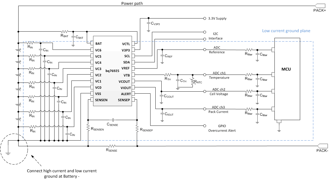
bq76925 layout_sep_gr_lusam9.gif Figure 22. Separate High-Current and Low-Current Grounds