JAJSBW2H November   2011  – June 2024 UCC27523 , UCC27525 , UCC27526

PRODUCTION DATA  

  1.   1
  2. 特長
  3. アプリケーション
  4. 概要
  5. 概要 (続き)
  6. Pin Configuration and Functions
  7. Specifications
    1. 6.1 Absolute Maximum Ratings
    2. 6.2 ESD Ratings
    3. 6.3 Recommended Operating Conditions
    4. 6.4 Thermal Information
    5. 6.5 Electrical Characteristics
    6. 6.6 Switching Characteristics
    7. 6.7 Typical Characteristics
  8. Detailed Description
    1. 7.1 Overview
    2. 7.2 Functional Block Diagrams
    3. 7.3 Feature Description
      1. 7.3.1 VDD and Undervoltage Lockout
      2. 7.3.2 Operating Supply Current
      3. 7.3.3 Input Stage
      4. 7.3.4 Enable Function
      5. 7.3.5 Output Stage
      6. 7.3.6 Low Propagation Delays and Tightly Matched Outputs
    4. 7.4 Device Functional Modes
  9. Application and Implementation
    1. 8.1 Application Information
    2. 8.2 Typical Application
      1. 8.2.1 Design Requirements
      2. 8.2.2 Detailed Design Procedure
        1. 8.2.2.1 Input-to-Output Logic
        2. 8.2.2.2 Enable and Disable Function
        3. 8.2.2.3 VDD Bias Supply Voltage
        4. 8.2.2.4 Propagation Delay
        5. 8.2.2.5 Drive Current and Power Dissipation
      3. 8.2.3 Application Curves
  10. Power Supply Recommendations
  11. 10Layout
    1. 10.1 Layout Guidelines
    2. 10.2 Layout Example
    3. 10.3 Thermal Considerations
  12. 11Device and Documentation Support
    1. 11.1 Device Support
      1. 11.1.1 サード・パーティ製品に関する免責事項
    2. 11.2 ドキュメントの更新通知を受け取る方法
    3. 11.3 サポート・リソース
    4. 11.4 Trademarks
    5. 11.5 静電気放電に関する注意事項
    6. 11.6 用語集
  13. 12Revision History
  14. 13Mechanical, Packaging, and Orderable Information

Functional Block Diagrams

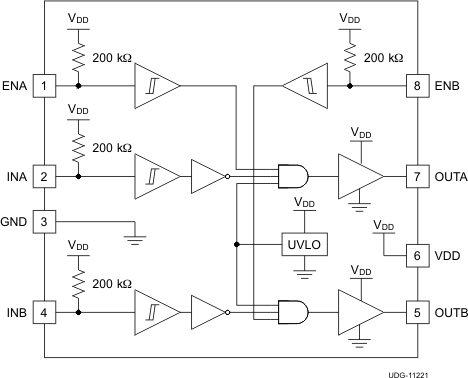
UCC27523 UCC27525 UCC27526 UCC27523 Block DiagramFigure 7-1 UCC27523 Block Diagram
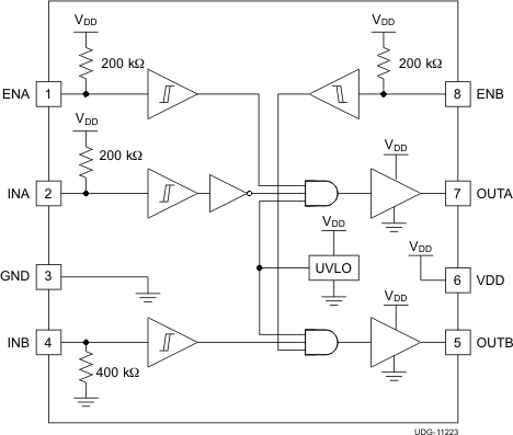
UCC27523 UCC27525 UCC27526 UCC27526 Block DiagramFigure 7-3 UCC27526 Block Diagram
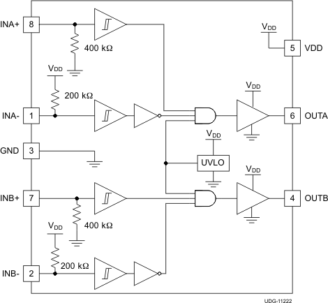
UCC27523 UCC27525 UCC27526 UCC27525 Block DiagramFigure 7-2 UCC27525 Block Diagram