JAJSCD9D July 2016 – December 2017 LM5141-Q1
PRODUCTION DATA.
- 1 特長
- 2 アプリケーション
- 3 概要
- 4 改訂履歴
- 5 Pin Configuration and Functions
- 6 Specifications
-
7 Detailed Description
- 7.1 Overview
- 7.2 Functional Block Diagram
- 7.3
Feature Description
- 7.3.1 High Voltage Start-up Regulator
- 7.3.2 VCC Regulator
- 7.3.3 Oscillator
- 7.3.4 Synchronization
- 7.3.5 Frequency Dithering (Spread Spectrum)
- 7.3.6 Enable
- 7.3.7 Power Good
- 7.3.8 Output Voltage
- 7.3.9 Current Sense
- 7.3.10 DCR Current Sensing
- 7.3.11 Error Amplifier and PWM Comparator
- 7.3.12 Slope Compensation
- 7.3.13 Hiccup Mode Current Limiting
- 7.3.14 Standby Mode
- 7.3.15 Soft Start
- 7.3.16 Diode Emulation
- 7.3.17 High- and Low-Side Drivers
-
8 Application and Implementation
- 8.1 Application Information
- 8.2 Typical Application
- 9 Power Supply Recommendations
- 10Layout
- 11デバイスおよびドキュメントのサポート
- 12メカニカル、パッケージ、および注文情報
8.2.2.5.4 Frequency Dithering
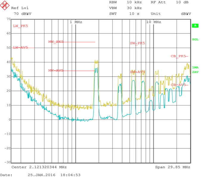
Figure 33 shows the CISPR 25 Class 5 conducted emission test run on the LM5141-Q1EVM, without the dither feature enabled. The first harmonic (peak measurement) is 48 dBµV, Figure 34 shows the conducted emissions test results with the dither feature enabled. With the dither featured enabled, the first harmonic (peak measurement) was lowered to 40 dBµV, an 8-dB reduction.
 Figure 33. CISPR 25 Class 5 Conducted EMI, Without Dither
 Figure 34. CISPR 25 Class 5 With Dither