JAJSCF6G July   2016  – December  2019 TPS2660

PRODUCTION DATA.  

  1. 特長
  2. アプリケーション
    1.     概略回路図
  3. 概要
    1.     -60V電源における入力逆極性保護
  4. 改訂履歴
  5. 概要(続き)
  6. Device Comparison Table
  7. Pin Configuration and Functions
    1.     Pin Functions
  8. Specifications
    1. 8.1 Absolute Maximum Ratings
    2. 8.2 ESD Ratings
    3. 8.3 Recommended Operating Conditions
    4. 8.4 Thermal Information
    5. 8.5 Electrical Characteristics
    6. 8.6 Timing Requirements
    7. 8.7 Typical Characteristics
  9. Parameter Measurement Information
  10. 10Detailed Description
    1. 10.1 Overview
    2. 10.2 Functional Block Diagram
    3. 10.3 Feature Description
      1. 10.3.1 Undervoltage Lockout (UVLO)
      2. 10.3.2 Overvoltage Protection (OVP)
      3. 10.3.3 Reverse Input Supply Protection
      4. 10.3.4 Hot Plug-In and In-Rush Current Control
      5. 10.3.5 Overload and Short Circuit Protection
        1. 10.3.5.1 Overload Protection
          1. 10.3.5.1.1 Active Current Limiting
          2. 10.3.5.1.2 Electronic Circuit Breaker with Overload Timeout, MODE = OPEN
        2. 10.3.5.2 Short Circuit Protection
          1. 10.3.5.2.1 Start-Up With Short-Circuit On Output
        3. 10.3.5.3 FAULT Response
          1. 10.3.5.3.1 Look Ahead Overload Current Fault Indicator
        4. 10.3.5.4 Current Monitoring
        5. 10.3.5.5 IN, OUT, RTN, and GND Pins
        6. 10.3.5.6 Thermal Shutdown
        7. 10.3.5.7 Low Current Shutdown Control (SHDN)
    4. 10.4 Device Functional Modes
  11. 11Application and Implementation
    1. 11.1 Application Information
    2. 11.2 Typical Application
      1. 11.2.1 Design Requirements
      2. 11.2.2 Detailed Design Procedure
        1. 11.2.2.1 Step by Step Design Procedure
        2. 11.2.2.2 Programming the Current-Limit Threshold—R(ILIM) Selection
        3. 11.2.2.3 Undervoltage Lockout and Overvoltage Set Point
        4. 11.2.2.4 Programming Current Monitoring Resistor—RIMON
        5. 11.2.2.5 Setting Output Voltage Ramp Time—(tdVdT)
          1. 11.2.2.5.1 Case 1: Start-Up Without Load—Only Output Capacitance C(OUT) Draws Current During Start-Up
          2. 11.2.2.5.2 Case 2: Start-Up With Load—Output Capacitance C(OUT) and Load Draws Current During Start-Up
          3. 11.2.2.5.3 Support Component Selections—RFLTb and C(IN)
      3. 11.2.3 Application Curves
    3. 11.3 System Examples
      1. 11.3.1 Acive ORing Operation
      2. 11.3.2 Field Supply Protection in PLC, DCS I/O Modules
      3. 11.3.3 Simple 24-V Power Supply Path Protection
    4. 11.4 Do's and Don'ts
  12. 12Power Supply Recommendations
    1. 12.1 Transient Protection
  13. 13Layout
    1. 13.1 Layout Guidelines
    2. 13.2 Layout Example
  14. 14デバイスおよびドキュメントのサポート
    1. 14.1 デバイス・サポート
    2. 14.2 ドキュメントのサポート
      1. 14.2.1 関連資料
    3. 14.3 ドキュメントの更新通知を受け取る方法
    4. 14.4 コミュニティ・リソース
    5. 14.5 商標
    6. 14.6 静電気放電に関する注意事項
    7. 14.7 Glossary
  15. 15メカニカル、パッケージ、および注文情報

Reverse Input Supply Protection

To protect the electronic systems from reverse input supply due to miswiring, often a power component like a schottky diode is added in series with the supply line as shown in Figure 35. These additional discretes result in a lossy and bulky protection solution. The TPS2660x devices feature fully integrated reverse input supply protection and does not need an additional diode. These devices can withstand –60 V reverse voltage without damage. Figure 36 illustrates the reverse input polarity protection functionality.

TPS2660 Application_Schematic_SLVSDG2.gifFigure 35. Reverse Input Supply Protection Circuits - Discrete vs TPS2660x
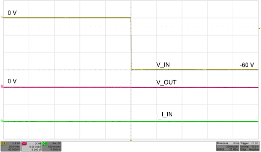
TPS2660 scope_shot_10_slvsdg2.gif
Figure 36. Reverse Input Supply Protection at –60 V