JAJSD52A March   2017  – December 2018 OPT3001-Q1

PRODUCTION DATA.  

  1. 特長
  2. アプリケーション
  3. 概要
    1.     ブロック図
    2.     スペクトル応答: OPT3001-Q1および肉眼
  4. 改訂履歴
  5. 概要(続き)
  6. Pin Configuration and Functions
    1.     Pin Functions
  7. Specifications
    1. 7.1 Absolute Maximum Ratings
    2. 7.2 ESD Ratings
    3. 7.3 Recommended Operating Conditions
    4. 7.4 Thermal Information
    5. 7.5 Electrical Characteristics
    6. 7.6 Timing Requirements
    7. 7.7 Typical Characteristics
  8. Detailed Description
    1. 8.1 Overview
    2. 8.2 Functional Block Diagram
    3. 8.3 Feature Description
      1. 8.3.1 Human Eye Matching
      2. 8.3.2 Automatic Full-Scale Range Setting
      3. 8.3.3 Interrupt Operation, INT Pin, and Interrupt Reporting Mechanisms
      4. 8.3.4 I2C Bus Overview
        1. 8.3.4.1 Serial Bus Address
        2. 8.3.4.2 Serial Interface
    4. 8.4 Device Functional Modes
      1. 8.4.1 Automatic Full-Scale Setting Mode
      2. 8.4.2 Interrupt Reporting Mechanism Modes
        1. 8.4.2.1 Latched Window-Style Comparison Mode
        2. 8.4.2.2 Transparent Hysteresis-Style Comparison Mode
        3. 8.4.2.3 End-of-Conversion Mode
        4. 8.4.2.4 End-of-Conversion and Transparent Hysteresis-Style Comparison Mode
    5. 8.5 Programming
      1. 8.5.1 Writing and Reading
        1. 8.5.1.1 High-Speed I2C Mode
        2. 8.5.1.2 General-Call Reset Command
        3. 8.5.1.3 SMBus Alert Response
    6. 8.6 Register Maps
      1. 8.6.1 Internal Registers
        1. 8.6.1.1 Register Descriptions
          1. 8.6.1.1.1 Result Register (offset = 00h)
            1. Table 7. Result Register Field Descriptions
          2. 8.6.1.1.2 Configuration Register (offset = 01h) [reset = C810h]
            1. Table 10. Configuration Register Field Descriptions
          3. 8.6.1.1.3 Low-Limit Register (offset = 02h) [reset = C0000h]
            1. Table 11. Low-Limit Register Field Descriptions
          4. 8.6.1.1.4 High-Limit Register (offset = 03h) [reset = BFFFh]
            1. Table 13. High-Limit Register Field Descriptions
          5. 8.6.1.1.5 Manufacturer ID Register (offset = 7Eh) [reset = 5449h]
            1. Table 14. Manufacturer ID Register Field Descriptions
          6. 8.6.1.1.6 Device ID Register (offset = 7Fh) [reset = 3001h]
            1. Table 15. Device ID Register Field Descriptions
  9. Application and Implementation
    1. 9.1 Application Information
      1. 9.1.1 Electrical Interface
      2. 9.1.2 Optical Interface
    2. 9.2 Typical Application
      1. 9.2.1 Design Requirements
      2. 9.2.2 Detailed Design Procedure
        1. 9.2.2.1 Optomechanical Design
        2. 9.2.2.2 Dark Window Selection and Compensation
      3. 9.2.3 Application Curves
    3. 9.3 Do's and Don'ts
  10. 10Power Supply Recommendations
  11. 11Layout
    1. 11.1 Layout Guidelines
    2. 11.2 Layout Example
  12. 12デバイスおよびドキュメントのサポート
    1. 12.1 ドキュメントのサポート
      1. 12.1.1 関連資料
    2. 12.2 ドキュメントの更新通知を受け取る方法
    3. 12.3 コミュニティ・リソース
    4. 12.4 商標
    5. 12.5 静電気放電に関する注意事項
    6. 12.6 Glossary
  13. 13メカニカル、パッケージ、および注文情報
    1. 13.1 ハンダ付けと取り扱いについての推奨事項
    2. 13.2 DNP (S-PDSO-N6)メカニカル図面

Typical Characteristics

At TA = 25°C, VDD = 3.3 V, 800-ms conversion time (CT = 1), automatic full-scale range (RN[3:0] = 1100b), white LED, and normal-angle incidence of light, unless otherwise specified.
OPT3001-Q1 D001_SBOS681.gif
Figure 2. Spectral Response vs Wavelength
OPT3001-Q1 D003_SBOS681.gif
Figure 4. Output Response vs Input Illuminance:
Entire Range = 0 lux to 83k lux
OPT3001-Q1 D005_SBOS681.gif
Figure 6. Output Response vs Input Illuminance:
Low Range = 0 lux to 5 lux
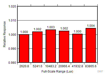
OPT3001-Q1 D007_SBOS681.gif
Input illuminance = 2490 lux,
normalized to response of 2560 lux full-scale
Figure 8. Full-Scale-Range Matching (Highest 6 Ranges)
OPT3001-Q1 D112-SBOS853.gif
Average of 30 devices
Figure 10. Dark Response vs Temperature (Grade 2)
OPT3001-Q1 D108-SBOS853.gif
Figure 12. Normalized Response vs Temperature (Grade 2)
OPT3001-Q1 D009_SBOS681.gif
Figure 14. Normalized Response vs Power-Supply Voltage
OPT3001-Q1 D011_SBOS681.gif
M[1:0] = 10b
Figure 16. Supply Current vs Input Illuminance
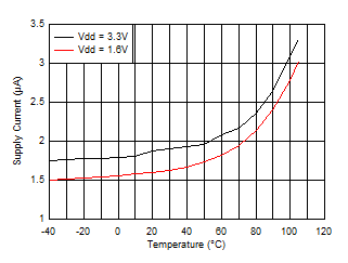
OPT3001-Q1 D110-SBOS853.gif
M[1:0] = 10b
Figure 18. Supply Current vs Temperature (Grade 2)
OPT3001-Q1 D111-SBOS853.gif
M[1:0] = 00b, input illuminance = 0 lux
Figure 20. Shutdown Current vs Temperature (Grade 2)
OPT3001-Q1 D015_SBOS681.gif
Input illuminance = 80 lux, SCL = SDA,
continuously toggled at I2C frequency
Note: A typical application runs at a lower duty cycle and thus consumes a lower current.
Figure 22. Supply Current vs Continuous I2C Frequency
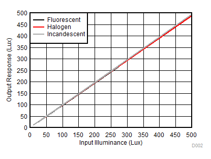
OPT3001-Q1 D002_SBOS681.gif
Figure 3. Output Response vs Input Illuminance, Multiple Light Sources: Fluorescent, Halogen, Incandescent
OPT3001-Q1 D004_SBOS681.gif
Figure 5. Output Response vs Input Illuminance:
Mid Range = 0 lux to 100 lux
OPT3001-Q1 D006_SBOS681.gif
Input illuminance = 33 lux,
normalized to response of 40.95 lux full-scale
Figure 7. Full-Scale-Range Matching: Lowest 7 Ranges
OPT3001-Q1 D017_SBOS681.gif
Figure 9. Conversion Time vs Power Supply
OPT3001-Q1 D016_SBOS681.gif
Average of 30 devices
Figure 11. Dark Response vs Temperature (Grade 3)
OPT3001-Q1 D008_SBOS681.gif
Figure 13. Normalized Response vs Temperature (Grade 3)
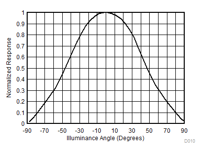
OPT3001-Q1 D010_SBOS681.gif
Figure 15. Normalized Response vs Illuminance Angle
OPT3001-Q1 D012_SBOS681.gif
M[1:0] = 00b
Figure 17. Shutdown Current vs Input Illuminance
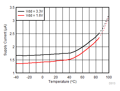
OPT3001-Q1 D013_SBOS681.gif
M[1:0] = 10b
Figure 19. Supply Current vs Temperature (Grade 3)
OPT3001-Q1 D014_SBOS681.gif
M[1:0] = 00b, input illuminance = 0 lux
Figure 21. Shutdown Current vs Temperature (Grade 3)