JAJSD96A February 2017 – June 2017 ADS114S06 , ADS114S08
PRODUCTION DATA.
- 1 特長
- 2 アプリケーション
- 3 概要
- 4 改訂履歴
- 5 Device Family Comparison Table
- 6 Pin Configuration and Functions
- 7 Specifications
- 8 Parameter Measurement Information
-
9 Detailed Description
- 9.1 Overview
- 9.2 Functional Block Diagram
- 9.3
Feature Description
- 9.3.1 Multiplexer
- 9.3.2 Low-Noise Programmable Gain Amplifier
- 9.3.3 Voltage Reference
- 9.3.4 Clock Source
- 9.3.5 Delta-Sigma Modulator
- 9.3.6 Digital Filter
- 9.3.7 Excitation Current Sources (IDACs)
- 9.3.8 Bias Voltage Generation
- 9.3.9 System Monitor
- 9.3.10 Status Register
- 9.3.11 General-Purpose Inputs and Outputs (GPIOs)
- 9.3.12 Low-Side Power Switch
- 9.3.13 Cyclic Redundancy Check (CRC)
- 9.3.14 Calibration
- 9.4 Device Functional Modes
- 9.5 Programming
- 9.6
Register Map
- 9.6.1
Configuration Registers
- 9.6.1.1 Device ID Register (address = 00h) [reset = xxh]
- 9.6.1.2 Device Status Register (address = 01h) [reset = 80h]
- 9.6.1.3 Input Multiplexer Register (address = 02h) [reset = 01h]
- 9.6.1.4 Gain Setting Register (address = 03h) [reset = 00h]
- 9.6.1.5 Data Rate Register (address = 04h) [reset = 14h]
- 9.6.1.6 Reference Control Register (address = 05h) [reset = 10h]
- 9.6.1.7 Excitation Current Register 1 (address = 06h) [reset = 00h]
- 9.6.1.8 Excitation Current Register 2 (address = 07h) [reset = FFh]
- 9.6.1.9 Sensor Biasing Register (address = 08h) [reset = 00h]
- 9.6.1.10 System Control Register (address = 09h) [reset = 10h]
- 9.6.1.11 Reserved Register (address = 0Ah) [reset = 00h]
- 9.6.1.12 Offset Calibration Register 1 (address = 0Bh) [reset = 00h]
- 9.6.1.13 Offset Calibration Register 2 (address = 0Ch) [reset = 00h]
- 9.6.1.14 Reserved Register (address = 0Dh) [reset = 00h]
- 9.6.1.15 Gain Calibration Register 1 (address = 0Eh) [reset = 00h]
- 9.6.1.16 Gain Calibration Register 2 (address = 0Fh) [reset = 40h]
- 9.6.1.17 GPIO Data Register (address = 10h) [reset = 00h]
- 9.6.1.18 GPIO Configuration Register (address = 11h) [reset = 00h]
- 9.6.1
Configuration Registers
- 10Application and Implementation
- 11Power Supply Recommendations
- 12Layout
- 13デバイスおよびドキュメントのサポート
- 14メカニカル、パッケージ、および注文情報
9 Detailed Description
9.1 Overview
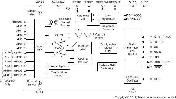
The ADS114S06 and ADS114S08 are precision 16-bit, delta-sigma (ΔΣ) ADCs with an integrated analog front end (AFE) to simplify precision sensor connections. The ADC provides output data rates from 2.5 SPS to 4000 SPS for flexibility in resolution and data rates over a wide range of applications. The low-noise and low-drift architecture make these devices suitable for precise measurement of low-voltage sensors, such as load cells and temperature sensors.
The ADS114S0x incorporate several features that simplify precision sensor measurements. Key integrated features include:
- Low-noise, CMOS PGA with integrated signal fault detection
- Low-drift, 2.5-V voltage reference
- Two sets of buffered external reference inputs with reference voltage level detection
- Dual, matched, sensor-excitation current sources (IDACs)
- Internal 4.096-MHz oscillator
- Temperature sensor
- Four general-purpose input/output pins (GPIOs)
- A low-resistance switch (when connected to AVSS) can be used to disconnect bridge sensors to reduce current consumption
As described in the Functional Block Diagram section, these devices provide 13 (ADS114S08) or 7 (ADS114S06) analog inputs that are configurable as either single-ended inputs, differential inputs, or any combination of the two. Many of the analog inputs have additional features as programmed by the user. The analog inputs can be programmed to enable the following extended features:
- Two sensor excitation current sources: all analog input pins (and REFP1 and REFN1 on the ADS114S06)
- Sensor biasing voltage (VBIAS): pins AIN0, AIN1, AIN2, AIN3, AIN4, AIN5, AINCOM
- Four GPIO pins: AIN8, AIN9, AIN10, AIN11 (ADS114S08 only, the ADS114S06 has dedicated GPIOs)
- Sensor burn-out current sources: analog input pins selected for ADC input
Following the input multiplexer (MUX), the ADC features a high input-impedance, low-noise, programmable gain amplifier (PGA), eliminating the need for an external amplifier. The PGA gain is programmable from 1 to 128 in binary steps. The PGA can be bypassed to allow the input range to extend 50 mV below ground or above supply. The PGA has output voltage monitors to verify the integrity of the conversion result.
An inherently stable delta-sigma modulator measures the ratio of the input voltage to the reference voltage to provide the ADC result. The ADC operates with the internal 2.5-V reference, or with up to two external reference inputs. The external reference inputs can be continuously monitored for low (or missing) voltage. The REFOUT pin provides the buffered 2.5-V internal voltage reference output that can be used to bias external circuitry.
The digital filter provides two filter modes, sinc3 and low-latency, allowing optimization of settling time and line-cycle rejection. The third-order sinc filter offers simultaneous 50-Hz and 60-Hz line-cycle rejection at data rates of 2.5 SPS, 5 SPS, and 10 SPS, 50-Hz rejection at data rates of 16.6 SPS and 50 SPS, and 60-Hz rejection at data rates of 20 SPS and 60 SPS. The low-latency filter provides settled data with 50-Hz and 60-Hz line-cycle rejection at data rates of 2.5 SPS, 5 SPS, 10 SPS, and 20 SPS, 50-Hz rejection at data rates of 16.6 SPS and 50 SPS, and 60-Hz rejection at a data rate of 60 SPS.
Two programmable excitation current sources provide bias to resistive sensors [such as resistance temperature detectors (RTDs) or thermistors]. The ADC integrates several system monitors for read back, such as temperature sensor and supply monitors. Four GPIO pins are available as either dedicated pins (ADS114S06) or combined with analog input pins (ADS114S08).
The ADS114S0x system clock is either provided by the internal low-drift, 4.096-MHz oscillator or an external clock source on the CLK input.
The SPI-compatible serial interface is used to read the conversion data and also to configure and control the ADC. The serial interface consists of four signals: CS, SCLK, DIN, and DOUT/DRDY. The conversion data are provided with an optional CRC code for improved data integrity. The dual function DOUT/DRDY output indicates when conversion data are ready and also provides the data output. The serial interface can be implemented with as little as three connections by tying CS low. Start ADC conversions with either the START/SYNC pin or with commands. The ADC can be programmed for a continuous conversion mode or to perform single-shot conversions.
The AVDD analog supply operates with bipolar supplies from ±1.5 V to ±2.625 V or with a unipolar supply from 2.7 V to 5.25 V. For unipolar-supply operation, use the VBIAS voltage to bias isolated (floating) sensors. The digital supplies operate with unipolar supplies only. The DVDD digital power supply operates from 2.7 V to 3.6 V and the IOVDD supply operates from DVDD to 5.25 V.
9.2 Functional Block Diagram
9.3 Feature Description
9.3.1 Multiplexer
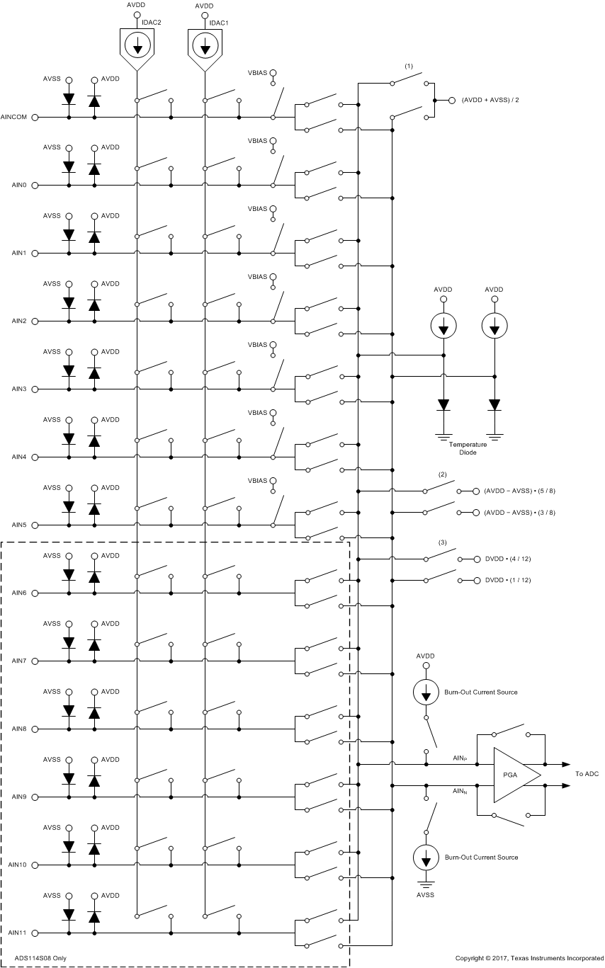
The ADS114S0x contains a flexible input multiplexer; see Figure 49. Select any of the six (ADS114S06) or 12 (ADS114S08) analog inputs as the positive or negative input for the PGA using the MUX_P[3:0] and MUX_N[3:0] bits in the input multiplexer register (02h). In addition, AINCOM can be selected as the positive or negative PGA input. AINCOM is treated as a regular analog input, as is AINx. Use AINCOM in single-ended measurement applications as the common input for the other analog inputs.
The multiplexer also routes the excitation current sources to drive resistive sensors (bridges, RTDs, and thermistors) and can provide bias voltages for unbiased sensors (unbiased thermocouples for example) to analog input pins.
The ADS114S0x also contain a set of system monitor functions measured through the multiplexer. The inputs can be shorted together at mid-supply [(AVDD + AVSS) / 2] to measure and calibrate the input offset of the analog front-end and the ADC. The system monitor also includes a temperature sensor that provides a measurement of the device temperature. The system monitor can also measure the analog and digital supplies, measuring [(AVDD – AVSS) / 4] for the analog supply or DVDD / 4 for the digital supply. Finally, the system monitor contains a set of burn-out current sources that pull the inputs to either supply if the sensor has burned out and has a high impedance so that the ADC measures a full-scale reading.
The multiplexer implements a break-before-make circuit. When changing the multiplexer channels using the MUX_P[3:0] and MUX_N[3:0] bits, the device first disconnects the PGA inputs from the analog inputs and connects them to mid-supply for 2 · tCLK. In the next step, the PGA inputs connect to the selected new analog input channels. This break-before-make behavior ensures the ADC always starts from a known state and that the analog inputs are not momentarily shorted together.
Electrostatic discharge (ESD) diodes to AVDD and AVSS protect the inputs. To prevent the ESD diodes from turning on, the absolute voltage on any input must stay within the range provided by Equation 3:
External Schottky clamp diodes or series resistors may be required to limit the input current to safe values (see the Absolute Maximum Ratings table). Overdriving an unselected input on the device can affect conversions taking place on other input pins.
9.3.2 Low-Noise Programmable Gain Amplifier
The ADS114S06 and ADS114S08 feature a low-drift, low-noise, high input impedance programmable gain amplifier (PGA). Figure 50 shows a simplified diagram of the PGA. The PGA consists of two chopper-stabilized amplifiers (A1 and A2) and a resistor feedback network that sets the gain of the PGA. The PGA input is equipped with an electromagnetic interference (EMI) filter and an antialiasing filter on the output.
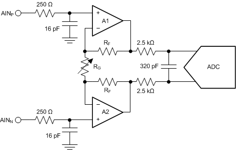 Figure 50. Simplified PGA Diagram
The PGA can be set to gains of 1, 2, 4, 8, 16, 32, 64, or 128 using the GAIN[2:0] bits in the gain setting register (03h). Gain is changed inside the device using a variable resistor, RG. The differential full-scale input voltage range (FSR) of the PGA is defined by the gain setting and the reference voltage used, as shown in Equation 4:
Table 9 shows the corresponding full-scale ranges when using the internal 2.5-V reference.
Table 9. PGA Full-Scale Range
| GAIN SETTING | FSR |
|---|---|
| 1 | ±2.5 V |
| 2 | ±1.25 V |
| 4 | ±0.625 V |
| 8 | ±0.313 V |
| 16 | ±0.156 V |
| 32 | ±0.078 V |
| 64 | ±0.039 V |
| 128 | ±0.020 V |
The PGA must be enabled with the PGA_EN[1:0] bits of the gain setting register (03h). Setting these bits to 00 powers down and bypasses the PGA. A setting of 01 enables the PGA. The 10 and 11 settings are reserved and must not be written to the device.
With the PGA enabled, gains 64 and 128 are established in the digital domain. When the device is set to 64 or 128, the PGA is set to a gain of 32, and additional gain is established with digital scaling. The input-referred noise does still improve compared to the gain = 32 setting because the PGA is biased with a higher supply current to reduce noise.
9.3.2.1 PGA Input-Voltage Requirements
As with many amplifiers, the PGA has an absolute input voltage range requirement that cannot be exceeded. The maximum and minimum absolute input voltages are limited by the voltage swing capability of the PGA output. The specified minimum and maximum absolute input voltages (VAINP and VAINN) depend on the PGA gain, the maximum differential input voltage (VINMAX), and the tolerance of the analog power-supply voltages (AVDD and AVSS). Use the maximum voltage expected in the application for VINMAX. The absolute positive and negative input voltages must be within the specified range, as shown in Equation 5:
where
- VAINP, VAINN = absolute input voltage
- VINMAX = VAINP – VAINN = maximum differential input voltage
As mentioned in the previous section, PGA gain settings of 64 and 128 are scaled in the digital domain and are not implemented with the amplifier. When using the PGA in gains of 64 and 128, set the gain in Equation 5 to 32 to calculate the absolute input voltage range.
The relationship between the PGA input to the PGA output is shown graphically in Figure 51. The PGA output voltages (VOUTP, VOUTN) depend on the PGA gain and the input voltage magnitudes. For linear operation, the PGA output voltages must not exceed AVDD – 0.15 V or AVSS + 0.15 V. Note that the diagram depicts a positive differential input voltage that results in a positive differential output voltage.
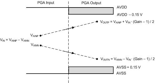 Figure 51. PGA Input/Output Range
Download the ADS1x4S0x design calculator from www.ti.com. This calculator can be used to determine the input voltage range of the PGA.
9.3.2.2 PGA Rail Flags
The PGA rail flags (FL_P_RAILP, FL_P_RAILN, FL_N_RAILP, and FL_N_RAILN) in the status register (01h) indicate if the positive or negative output of the PGA is closer to the analog supply rails than 150 mV. Enable the PGA output rail detection circuit using the FL_RAIL_EN bit in the excitation current register 1 (06h). A flag going high indicates that the PGA is operating outside the linear operating or absolute input voltage range. PGA rail flags are discussed in more detail in the PGA Output Voltage Rail Monitors section.
9.3.2.3 Bypassing the PGA
At a gain of 1, the device can be configured to disable and bypass the low-noise PGA. Disabling the PGA lowers the overall power consumption and also removes the restrictions of Equation 5 for the input voltage range. If the PGA is bypassed, the ADC absolute input voltage range extends beyond the AVDD and AVSS power supplies, allowing input voltages at or below ground. The absolute input voltage range when the PGA is bypassed is shown in Equation 6:
In order to measure single-ended signals that are referenced to AVSS (AINP = VIN, AINN = AVSS), the PGA must be bypassed. The PGA is bypassed and powered down by setting the PGA_EN[1:0] bits to 00 in the gain setting register (03h).
For signal sources with high output impedance, external buffering may still be necessary. Note that active buffers introduce noise and also introduce offset and gain errors. Consider all of these factors in high-accuracy applications.
9.3.3 Voltage Reference
The devices require a reference voltage for operation. The ADS114S0x offers an integrated low-drift 2.5-V reference. For applications that require a different reference voltage value or a ratiometric measurement approach, the ADS114S08 offers two differential reference input pairs (REFP0, REFN0 and REFP1, REFN1). The differential reference inputs allow freedom in the reference common-mode voltage. REFP0 and REFN0 are dedicated reference inputs, whereas REFP1 and REFN1 are shared with inputs AIN6 and AIN7 (respectively) on the ADS114S08. The specified external reference voltage range is 0.5 V to AVDD. The reference voltage is shown in Equation 7, where V(REFPx) and V(REFNx) are the absolute positive and absolute negative reference voltages.
The polarity of the reference voltage internal to the ADC must be positive. The magnitude of the reference voltage together with the PGA gain establishes the ADC full-scale differential input range as defined by
FSR = ±VREF / Gain.
Figure 52 shows the block diagram of the reference multiplexer. The ADC reference multiplexer selects between the internal reference and two external references (REF0 and REF1). The reference multiplexer is programmed with the REFSEL[1:0] bits in the reference control register (05h). By default, the external reference pair REFP0, REFN0 is selected.
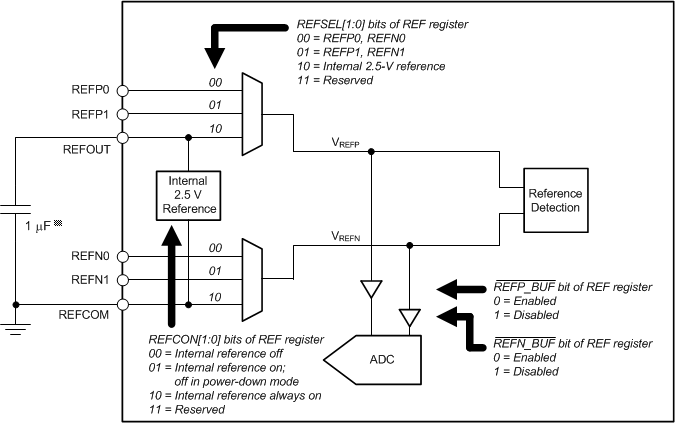
The ADC also contains an integrated reference voltage monitor. This monitor provides continuous detection of a low or missing reference during the conversion cycle. The reference monitor flags (FL_REF_L0 and FL_REF_L1) are set in the STATUS byte and described in the Reference Monitor section.
9.3.3.1 Internal Reference
The ADC integrates a precision, low-drift, 2.5-V reference. The internal reference is enabled by setting REFCON[1:0] to 10 (reference is always on) or 01 (reference is on, but powers down in power-down mode) in the reference control register (05h). By default, the internal voltage reference is powered down. To select the internal reference for use with the ADC, set the REFSEL[1:0] bits to 10. The REFOUT pin provides a buffered reference output voltage when the internal reference voltage is enabled. The negative reference output is the REFCOM pin, as shown in Figure 52. Connect a capacitor in the range of 1 μF to 47 μF between REFOUT and REFCOM. Larger capacitor values help filter more noise at the expense of a longer reference start-up time.
The capacitor is not required if the internal reference is not used. However, the internal reference must be powered on if using the IDACs.
The internal reference requires a start-up time that must be accounted for before starting a conversion, as shown in Table 10.
Table 10. Internal Reference Settling Time
| REFOUT CAPACITOR | SETTLING ERROR | SETTLING TIME (ms) |
|---|---|---|
| 1 µF | 0.01% | 4.5 |
| 0.001% | 5.9 | |
| 10 µF | 0.01% | 4.9 |
| 0.001% | 6.3 | |
| 47 µF | 0.01% | 5.5 |
| 0.001% | 7.0 |
9.3.3.2 External Reference
The ADS114S0x provides two external reference inputs selectable through the reference multiplexer. The reference inputs are differential with independent positive and negative inputs. REFP0 and REFN0 or REFP1 and REFN1 can be selected as the ADC reference. REFP1 and REFN1 are shared inputs with analog pins AIN6 and AIN7 in the ADS114S08.
Without buffering, the reference input impedance is approximately 250 kΩ. The reference input current can lead to possible errors from either high reference source impedance or through reference input filtering. To reduce the input current, use either internal or external reference buffers. In most applications external reference buffering is not necessary.
Connect a 100-nF bypass capacitor across the external reference input pins. Follow the specified absolute and differential reference voltage requirements.
9.3.3.3 Reference Buffers
The device has two individually selectable reference input buffers to lower the reference input current. Use the REFP_BUF and REFN_BUF bits in the reference control register (05h) to enable or disable the positive and negative reference buffers respectively. Note that these bits are active low. Writing a 1 to REFP_BUF or REFN_BUF disables the reference buffers.
The reference buffers are recommended to be disabled when the internal reference is selected for measurements. When the external reference input is at the supply voltage (REFPx at AVDD or REFNx at AVSS), the reference buffer is recomended to be disabled.
9.3.4 Clock Source
The ADS114S0x system clock is either provided by the internal low-drift 4.096-MHz oscillator or an external clock source on the CLK input. Use the CLK bit within the data rate register (04h) to select the internal
4.096-MHz oscillator or an external clock source.
The device defaults to using the internal oscillator. If the device is reset (from either the RESET pin, or the RESET command), then the clock source returns to using the internal oscillator even if an external clock is selected.
9.3.5 Delta-Sigma Modulator
A delta-sigma (ΔΣ) modulator is used in the devices to convert the analog input voltage into a pulse code modulated (PCM) data stream. The modulator runs at a modulator clock frequency of fMOD = fCLK / 16, where fCLK is either provided by the internal 4.096-MHz oscillator or the external clock source.
9.3.6 Digital Filter
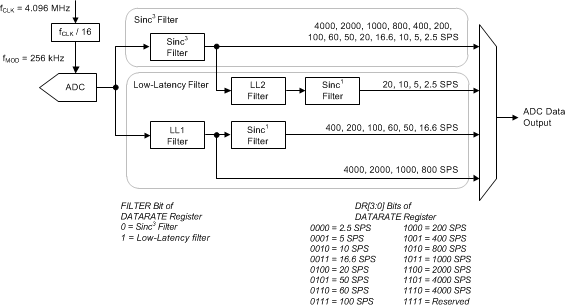
The devices offer digital filter options for both filtering and decimation of the digital data stream coming from the delta-sigma modulator. The implementation of the digital filter is determined by the data rate and filter mode setting. Figure 53 shows the digital filter implementation. Choose between a third-order sinc filter (sinc3) and a low-latency filter (low-latency filter with multiple components) using the FILTER bit in the data rate register (04h).
NOTE:
LL filter = low-latency filter.Regardless of the FILTER type setting, the oversampling ratio is the same for each given data rate, meaning that the device requires a set number of modulator clocks to output a single ADC conversion data. The output data rate is selected using the DR[3:0] bits in the data rate register and is shown in Table 11.
Table 11. ADC Data Rates and Digital Filter Oversampling Ratios
| NOMINAL DATA RATE (SPS)(1) |
DATA RATE REGISTER DR[3:0] |
OVERSAMPLING RATIO(2) |
|---|---|---|
| 2.5 | 0000 | 102400 |
| 5 | 0001 | 51200 |
| 10 | 0010 | 25600 |
| 16.6 | 0011 | 15360 |
| 20 | 0100 | 12800 |
| 50 | 0101 | 5120 |
| 60 | 0110 | 4264 |
| 100 | 0111 | 2560 |
| 200 | 1000 | 1280 |
| 400 | 1001 | 640 |
| 800 | 1010 | 320 |
| 1000 | 1011 | 256 |
| 2000 | 1100 | 128 |
| 4000 | 1101 | 64 |
9.3.6.1 Low-Latency Filter
The low-latency filter is selected when the FILTER bit is set to 0 in the data rate register (04h). The filter is a finite impulse response (FIR) filter that provides settled data, given that the analog input signal has settled to the final value before the conversion is started. The low-latency filter is especially useful when multiple channels must be scanned in minimal time.
9.3.6.1.1 Low-Latency Filter Frequency Response
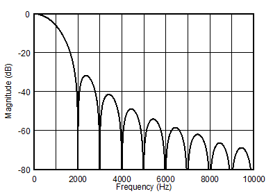
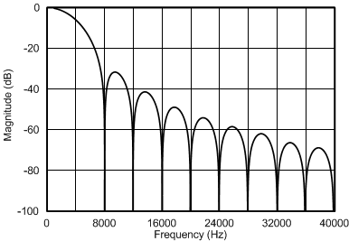
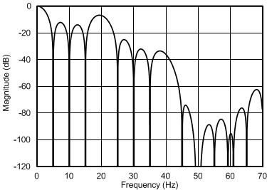
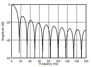
The low-latency filter provides many data rate options for rejecting 50-Hz and 60-Hz line cycle noise. At data rates of 2.5 SPS, 5 SPS, 10 SPS, and 20 SPS, the filter rejects both 50-Hz and 60-Hz line frequencies. At data rates of 16.6 SPS and 50 SPS, the filter has a notch at 50 Hz. At a 60-SPS data rate, the filter has a notch at 60 Hz.
For detailed frequency response plots showing line cycle noise rejection, download the ADS1x4S0x design calculator from www.ti.com.
Figure 54 to Figure 68 show the frequency response of the low-latency filter for different data rates. Table 12 gives the bandwidth of the low-latency filter for each data rate.
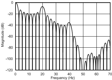
| fCLK = 4.096 MHz, low-latency filter |
Data Rate = 2.5 SPS
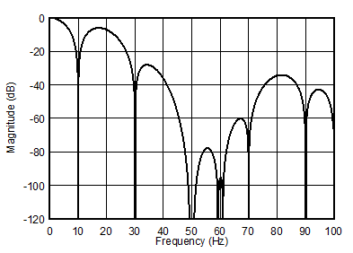
| fCLK = 4.096 MHz, low-latency filter |
Data Rate = 10 SPS
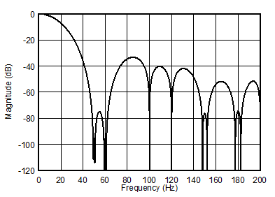
| fCLK = 4.096 MHz, low-latency filter |
Data Rate = 20 SPS
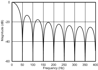
| fCLK = 4.096 MHz, low-latency filter |
Data Rate = 50 SPS
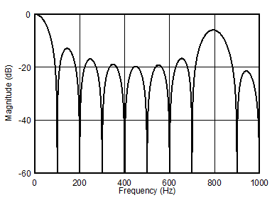
| fCLK = 4.096 MHz, low-latency filter |
Data Rate = 100 SPS
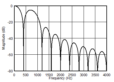
| fCLK = 4.096 MHz, low-latency filter |
Data Rate = 400 SPS
| fCLK = 4.096 MHz, low-latency filter |
Data Rate = 1 kSPS
| fCLK = 4.096 MHz, low-latency filter |
Data Rate = 4 kSPS
| fCLK = 4.096 MHz, low-latency filter |
Data Rate = 5 SPS
| fCLK = 4.096 MHz, low-latency filter |
Data Rate = 16.6 SPS
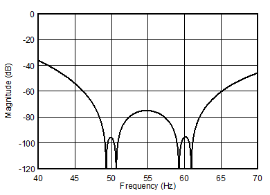
| fCLK = 4.096 MHz, low-latency filter |
Data Rate = 20 SPS, Zoomed to 50 Hz and 60 Hz
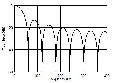
| fCLK = 4.096 MHz, low-latency filter |
Data Rate = 60 SPS
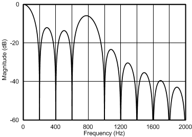
| fCLK = 4.096 MHz, low-latency filter |
Data Rate = 200 SPS
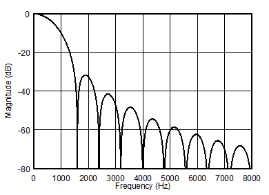
| fCLK = 4.096 MHz, low-latency filter |
Data Rate = 800 SPS
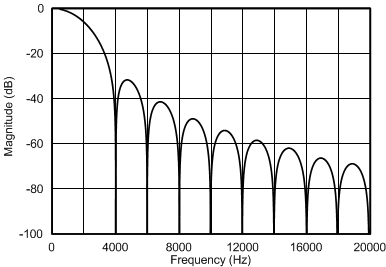
| fCLK = 4.096 MHz, low-latency filter |
Data Rate = 2 kSPS
Table 12. Low-Latency Filter Bandwidth
| NOMINAL DATA RATE (SPS)(1) | –3-dB BANDWIDTH (Hz)(1) |
|---|---|
| 2.5 | 1.1 |
| 5 | 2.2 |
| 10 | 4.7 |
| 16.6 | 7.4 |
| 20 | 13.2 |
| 50 | 22.1 |
| 60 | 26.6 |
| 100 | 44.4 |
| 200 | 89.9 |
| 400 | 190 |
| 800 | 574 |
| 1000 | 718 |
| 2000 | 718 |
| 4000 | 718 |
The low-latency filter notches and output data rate scale proportionally with the clock frequency. For example, a notch that appears at 20 Hz when using a 4.096-MHz clock appears at 10 Hz if a 2.048-MHz clock is used. Note that the internal oscillator can vary over temperature as specified in the Electrical Characteristics table. The data rate, conversion time, and filter notches consequently vary by the same percentage. Consider using an external precision clock source if a digital filter notch at a specific frequency with a tighter tolerance is required.
9.3.6.1.2 Data Conversion Time for the Low-Latency Filter
The amount of time required to receive data from the ADC depends on more than just the nominal data rate of the device. The data period also depends on the mode of operation and other configurations of the device. When the low-latency filter is enabled, the data settles in one data period. However, a small amount of latency exists to set up the device, calculate the conversion data from the modulator samples, and other overhead that adds time to the conversion. For this reason, the first conversion data takes longer than subsequent data conversions.
Table 13 shows the conversion times for the low-latency filter for each ADC data rate and various conversion modes.
Table 13. Data Conversion Time for the Low-Latency Filter
| NOMINAL DATA RATE(1) (SPS) |
FIRST DATA FOR CONTINUOUS CONVERSION MODE OR SINGLE-SHOT CONVERSION MODE(2) |
SECOND AND SUBSEQUENT CONVERSIONS FOR CONTINUOUS CONVERSION MODE |
||
|---|---|---|---|---|
| ms(3) | NUMBER OF tMOD PERIODS(3) |
ms(4) | NUMBER OF tMOD PERIODS(4) |
|
| 2.5 | 406.504 | 104065 | 400 | 102400 |
| 5 | 206.504 | 52865 | 200 | 51200 |
| 10 | 106.504 | 27265 | 100 | 25600 |
| 16.6 | 60.254 | 15425 | 60 | 15360 |
| 20 | 56.504 | 14465 | 50 | 12800 |
| 50 | 20.156 | 5160 | 20 | 5120 |
| 60 | 16.910 | 4329 | 16.66 | 4264 |
| 100 | 10.156 | 2600 | 10 | 2560 |
| 200 | 5.156 | 1320 | 5 | 1280 |
| 400 | 2.656 | 680 | 2.5 | 640 |
| 800 | 1.406 | 360 | 1.25 | 320 |
| 1000 | 1.156 | 296 | 1 | 256 |
| 2000 | 0.656 | 168 | 0.5 | 128 |
| 4000 | 0.406 | 104 | 0.25 | 64 |
9.3.6.2 Sinc3 Filter
The sinc3 digital filter is selected when the FILTER bit is set to 0 in the data rate register (04h). Compared to the low-latency filter, the sinc3 filter has improved noise performance but has a three-cycle latency in the data output.
9.3.6.2.1 Sinc3 Filter Frequency Response
The low-pass nature of the sinc3 filter establishes the overall frequency response. The frequency response is given by Equation 8:

where
- f = signal frequency
- fCLK = ADC clock frequency
- OSR = oversampling ratio
The sinc3 filter offers simultaneous 50-Hz and 60-Hz line cycle rejection at data rates of 2.5 SPS, 5 SPS, and 10 SPS. The sinc3 filter offers only 50-Hz rejection at data rates of 16.6 SPS and 50 SPS, and only 60-Hz rejection at data rates of 20 SPS and 60 SPS. The sinc3 digital filter response scales with the data rate and has notches at multiples of the data rate. Figure 69 shows the sinc3 digital filter frequency response normalized to the data rate. As an example, Figure 70 shows the frequency response when the data rate is set to 10 SPS, and Figure 71 illustrates a close-up of the filter rejection of 50-Hz and 60-Hz line frequencies. For more detailed frequency response plots, download the ADS1x4S0x design calculator from www.ti.com.
Table 14 gives the bandwidth of the sinc3 filter for each data rate.
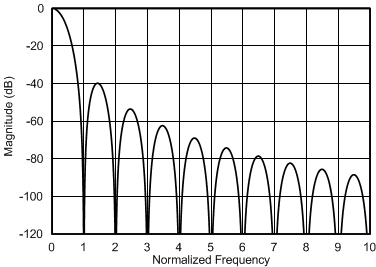
| Frequency normalized to data rate, sinc3 filter |
Normalized to Data Rate
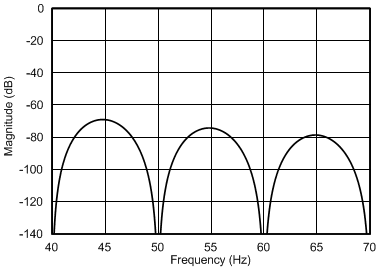
| fCLK = 4.096 MHz, sinc3 filter |
Data Rate = 10 SPS, Zoomed to 50 Hz and 60 Hz
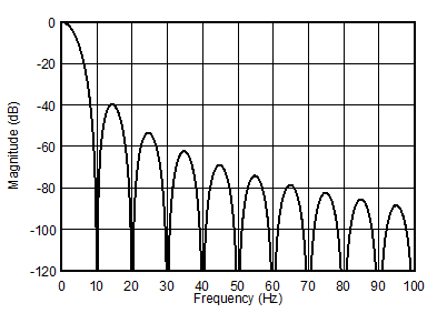
| fCLK = 4.096 MHz, sinc3 filter |
Data Rate = 10 SPS
Table 14. Sinc3 Filter –3-dB Bandwidth
| NOMINAL DATA RATE (SPS)(1) | –3-dB BANDWIDTH (Hz)(1) |
|---|---|
| 2.5 | 0.65 |
| 5 | 1.3 |
| 10 | 2.6 |
| 16.6 | 4.4 |
| 20 | 5.2 |
| 50 | 13.1 |
| 60 | 15.7 |
| 100 | 26.2 |
| 200 | 52.3 |
| 400 | 105 |
| 800 | 209 |
| 1000 | 262 |
| 2000 | 523 |
| 4000 | 1046 |
As mentioned in the previous section, filter notches and output data rate scale proportionally with the clock frequency and the internal oscillator can change frequency with temperature.
9.3.6.2.2 Data Conversion Time for the Sinc3 Filter
Similar to the low-latency filter, the sinc3 filter requires different amounts of time to complete a conversion. By nature, the sinc3 filter normally takes three conversion to settle. In both single-shot conversion mode and continuous conversion mode, the first two conversions are suppressed so that only settled data are output by the ADC.
Table 15 shows the conversion times for the sinc3 filter for each ADC data rate and various conversion modes.
Table 15. Data Conversion Time for the Sinc3 Filter
| NOMINAL DATA RATE(1) (SPS) | FIRST DATA FOR CONTINUOUS CONVERSION MODE OR SINGLE-SHOT CONVERSION MODE(2) |
SECOND AND SUBSEQUENT CONVERSIONS FOR CONTINUOUS CONVERSION MODE |
||
|---|---|---|---|---|
| ms(3) | NUMBER OF tMOD PERIODS(3) |
ms(4) | NUMBER OF tMOD PERIODS(4) |
|
| 2.5 | 1200.254 | 307265 | 400 | 102400 |
| 5 | 600.254 | 153665 | 200 | 51200 |
| 10 | 300.254 | 76865 | 100 | 25600 |
| 16.6 | 180.254 | 46145 | 60 | 15360 |
| 20 | 150.254 | 38465 | 50 | 12800 |
| 50 | 60.254 | 15425 | 20 | 5120 |
| 60 | 50.223 | 12857 | 16.66 | 4264 |
| 100 | 30.254 | 7745 | 10 | 2560 |
| 200 | 15.254 | 3905 | 5 | 1280 |
| 400 | 7.754 | 1985 | 2.5 | 640 |
| 800 | 4.004 | 1025 | 1.25 | 320 |
| 1000 | 3.156 | 808 | 1 | 256 |
| 2000 | 1.656 | 424 | 0.5 | 128 |
| 4000 | 0.906 | 232 | 0.25 | 64 |
9.3.6.3 Note on Conversion Time
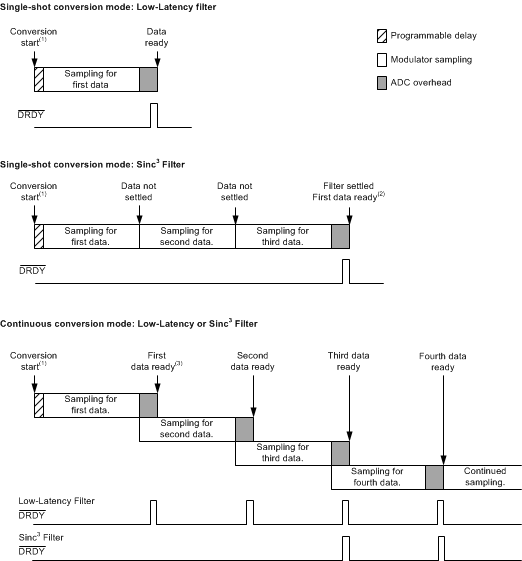
Each data period consists of time required for the modulator to sample the analog inputs. However, there is additional time required before the samples become an ADC conversion result. First, there is a programmable conversion delay (described in the Programmable Conversion Delay section) that is added before the conversion starts. This delay allows for additional settling time for input filtering on the analog inputs and for the antialiasing filter after the PGA. The default programmable conversion delay is 14 · tMOD. Also, overhead time is needed to convert the modulator samples into an ADC conversion result. This overhead time includes any necessary offset or gain compensation after the digital filter accumulates a data result.
The first conversion when the device is in continuous conversion mode (just as in single-shot conversion mode) includes the programmable conversion delay, the modulator sampling time, and the overhead time. The second and subsequent conversions are the normal data period (period as given by the inverse of the data rate).
Figure 72 shows the time sequence for the ADC in both continuous conversion and single-shot conversion modes. The sequence is the same regardless of the filter setting. However, when the low-latency filter settles for each data, the sinc3 filter does not settle until the third data.
9.3.6.4 50-Hz and 60-Hz Line Cycle Rejection
If the ADC connection leads are in close proximity to industrial motors and conductors, coupling of 50-Hz and
60-Hz power line frequencies can occur. The coupled noise interferes with the signal voltage, and can lead to inaccurate or unstable conversions. The digital filter provides enhanced rejection of power-line-coupled noise for data rates of 60 SPS and less. Program the filter to tradeoff data rate and conversion latency versus the desired level of line cycle rejection. Table 16 and Table 17 summarize the ADC 50-Hz and 60-Hz line-cycle rejection based on ±1-Hz and ±2-Hz tolerance of power-line to ADC clock frequency. The best possible power-line rejection is provided by using an accurate ADC clock.
Table 16. Low-Latency Filter, 50-Hz and 60-Hz Line Cycle Rejection
| DATA RATE (SPS)(1) | LOW-LATENCY DIGITAL FILTER LINE CYCLE REJECTION (dB) | |||
|---|---|---|---|---|
| 50 Hz ± 1 Hz | 60 Hz ± 1 Hz | 50 Hz ± 2 Hz | 60 Hz ± 2 Hz | |
| 2.5 | –113.7 | –95.4 | –97.7 | –92.4 |
| 5 | –111.9 | –95.4 | –87.6 | –81.8 |
| 10 | –111.5 | –95.4 | –85.7 | –81.0 |
| 16.6 | –33.8 | –20.9 | –27.8 | –20.8 |
| 20 | –95.4 | –95.4 | –75.5 | –80.5 |
| 50 | –33.8 | –15.5 | –27.6 | –15.1 |
| 60 | –13.4 | –35.0 | –12.6 | –29.0 |
Table 17. Sinc3 Filter, 50-Hz and 60-Hz Line Cycle Rejection
| DATA RATE (SPS)(1) | SINC3 DIGITAL FILTER LINE CYCLE REJECTION (dB) | |||
|---|---|---|---|---|
| 50 Hz ± 1 Hz | 60 Hz ± 1 Hz | 50 Hz ± 2 Hz | 60 Hz ± 2 Hz | |
| 2.5 | –108.7 | –113.4 | –107.2 | –112.1 |
| 5 | –103.2 | –107.8 | –90.1 | –95.0 |
| 10 | –101.8 | –106.4 | –84.6 | –89.4 |
| 16.6 | –101.6 | –63.0 | –83.4 | –62.4 |
| 20 | –53.5 | –106.1 | –53.5 | –88.0 |
| 50 | –101.4 | –46.7 | –82.9 | –45.3 |
| 60 | –40.3 | –105.1 | –37.8 | –87.2 |
9.3.6.5 Global Chop Mode
The device uses a very low-drift PGA and modulator in order to provide very low input voltage offset drift. However, a small amount of offset voltage drift sometimes remains in normal measurement. The ADC incorporates a global chop option to reduce the offset voltage and offset voltage drift to very low levels. When the global chop is enabled, the ADC performs two internal conversions to cancel the input offset voltage. The first conversion is taken with normal input polarity. The ADC reverses the internal input polarity for a second conversion. The average of the two conversions yields the final corrected result, removing the offset voltage. The global chop mode is enabled using the G_CHOP bit in the data rate register (04h). Figure 73 shows a block diagram of the global chop implementation. The combined PGA and ADC internal offset voltage is modeled as VOFS.
 Figure 73. ADC Global Chop Block Diagram
The first conversion result is available after the ADC takes two separate conversions with settled data. When using the low-latency filter, data settles in a single conversion. When the global chop mode is enabled, the first conversion result appears after a time period of approximately two conversions. When using the sinc3 filter, data settles in three conversions. If the global chop mode is enabled, the first conversion result appears after a time period of approximately six conversions.
In continuous conversion mode with the global chop mode enabled, subsequent conversions complete in half the time as the first conversion completed. Data for alternating inputs are pipelined so that averaging appears on each ADC data cycle. Conversion times using the global chop mode are given in Table 18 and Table 19.
Table 18. Data Conversion Time for Global Chop Mode Using the Low-Latency Filter
| NOMINAL DATA RATE(1) (SPS) |
FIRST DATA CONVERSION PERIOD FOR GLOBAL CHOP MODE(2) |
SECOND AND SUBSEQUENT CONVERSION PERIODS FOR GLOBAL CHOP MODE |
||
|---|---|---|---|---|
| ms(3) | NUMBER OF tMOD PERIODS(3) |
ms(3) | NUMBER OF tMOD PERIODS(3) |
|
| 2.5 | 813.008 | 208130 | 406.504 | 104065 |
| 5 | 413.008 | 105730 | 206.504 | 52865 |
| 10 | 213.008 | 54530 | 106.504 | 27265 |
| 16.66 | 120.508 | 30850 | 60.254 | 15425 |
| 20 | 113.008 | 28930 | 56.504 | 14465 |
| 50 | 40.313 | 10320 | 20.156 | 5160 |
| 60 | 33.820 | 8658 | 16.910 | 4329 |
| 100 | 20.313 | 5200 | 10.156 | 2600 |
| 200 | 10.313 | 2640 | 5.156 | 1320 |
| 400 | 5.313 | 1360 | 2.656 | 680 |
| 800 | 2.813 | 720 | 1.406 | 360 |
| 1000 | 2.313 | 592 | 1.156 | 296 |
| 2000 | 1.313 | 336 | 0.656 | 168 |
| 4000 | 0.813 | 208 | 0.406 | 104 |
Table 19. Data Conversion Time for Global Chop Mode Using the Sinc3 Filter
| NOMINAL DATA RATE(1) (SPS) |
FIRST DATA CONVERSION PERIOD FOR GLOBAL CHOP MODE(2) |
SECOND AND SUBSEQUENT CONVERSION PERIODS FOR GLOBAL CHOP MODE |
||
|---|---|---|---|---|
| ms(3) | NUMBER OF tMOD PERIODS(3) | ms(3) | NUMBER OF tMOD PERIODS(3) | |
| 2.5 | 2400.508 | 614530 | 1200.254 | 307265 |
| 5 | 1200.508 | 307330 | 600.254 | 153665 |
| 10 | 600.508 | 153730 | 300.254 | 76865 |
| 16.66 | 360.508 | 92290 | 180.254 | 46145 |
| 20 | 300.508 | 76930 | 150.254 | 38465 |
| 50 | 120.508 | 30850 | 60.254 | 15425 |
| 60 | 100.445 | 25714 | 50.223 | 12857 |
| 100 | 60.508 | 15490 | 30.254 | 7745 |
| 200 | 30.508 | 7810 | 15.254 | 3905 |
| 400 | 15.508 | 3970 | 7.754 | 1985 |
| 800 | 8.008 | 2050 | 4.004 | 1025 |
| 1000 | 6.313 | 1616 | 3.156 | 808 |
| 2000 | 3.313 | 848 | 1.656 | 424 |
| 4000 | 1.813 | 464 | 0.906 | 232 |
In global chop mode, sequences are similar to taking consecutive single-shot conversions and swapping the input on each conversion. Output data are averaged using the last two data read operations by the ADC with the inputs swapped. Figure 74 shows the time sequence for the ADC using global chop mode.
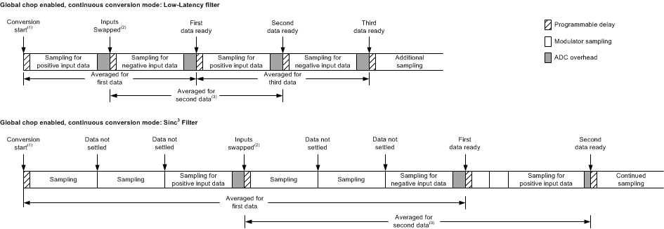
Because the digital filter must settle after reversing the inputs, the global chop mode data rate is less than the nominal data rate, depending on the digital filter and programmed settling delay. However, if the data rate in use has 50-Hz and 60-Hz frequency response notches, the null frequencies remain unchanged.
The global chop mode also reduces the ADC noise by a factor of √2 because two conversions are averaged. In some cases, the programmable conversion delay must be increased, DELAY[2:0] in the gain setting register (03h), to allow for settling of external components.
9.3.7 Excitation Current Sources (IDACs)
The ADS114S0x incorporates two integrated, matched current sources (IDAC1, IDAC2). The current sources provide excitation current to resistive temperature devices (RTDs), thermistors, diodes, and other resistive sensors that require constant current biasing. The current sources are programmable to output values between 10 μA to 2000 μA using the IMAG[3:0] bits in the excitation current register 1 (06h). Each current source can be connected to any of the analog inputs AINx as well as the REFP1 and REFN1 inputs for the ADS114S06. Both current sources can also be connected to the same pin. The routing of the IDACs is configured by the I1MUX[3:0] and I2MUX[3:0] bits in the excitation current register 2 (07h). In three-wire RTD applications, the matched current sources can be used to cancel errors caused by sensor lead resistance (see the Typical Application section for more details). Figure 75 details the IDAC connection through the input multiplexer.
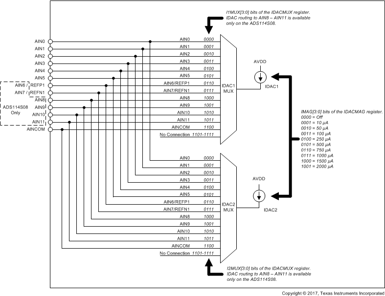 Figure 75. IDAC Block Diagram
The internal reference must be enabled for IDAC operation. As a current source, the IDAC requires voltage headroom to the positive supply to operate. This voltage headroom is the compliance voltage. When driving resistive sensors and biasing resistors, take care not to exceed the compliance voltage of the IDACs, otherwise the specified accuracy of the IDAC current may not be met. For IDAC compliance voltage specifications, see the Electrical Characteristics table.
9.3.8 Bias Voltage Generation
The ADS114S0x provides an internal bias voltage generator, VBIAS, that can be set to two different levels,
(AVDD + AVSS) / 2 and (AVDD + AVSS) / 12 by using the VB_LEVEL bit in the sensor biasing register (08h). The bias voltage is internally buffered and can be established on the analog inputs AIN0 to AIN5 and AINCOM using the VB_AINx bits in the sensor biasing register (08h). A typical use case for VBIAS is biasing unbiased thermocouples to within the common-mode voltage range of the PGA. A block diagram of the VBIAS voltage generator and connection diagram is shown in Figure 76.
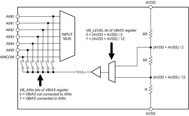 Figure 76. VBIAS Block Diagram
The start-up time of the VBIAS voltage depends on the pin load capacitance. The total capacitance includes any capacitance connected from VBIAS to AVDD, AVSS, and ground. Table 20 lists the VBIAS voltage settling times for various external load capacitances. Ensure the VBIAS voltage is fully settled before starting a conversion.
Table 20. VBIAS Settling Time
| LOAD CAPACITANCE | SETTLING TIME |
|---|---|
| 0.1 µF | 280 µs |
| 1 µF | 2.8 ms |
| 10 µF | 28 ms |
9.3.9 System Monitor
The ADS114S0x provides a set of system monitor functions. These functions measure the device temperature, analog power supply, digital power supply, or use current sources to detect sensor malfunction. System monitor functions are enabled through the SYS_MON[2:0] bits of the system control register (09h).
9.3.9.1 Internal Temperature Sensor
On-chip diodes provide temperature-sensing capability. Enable the internal temperature sensor by setting SYS_MON[2:0] = 010 in the system control register (09h). The temperature sensor outputs a voltage proportional to the device temperature as specified in the Electrical Characteristics table.
When measuring the internal temperature sensor, the analog inputs are disconnected from the ADC and the output voltage of the temperature sensor is routed to the ADC for measurement using the selected PGA gain, data rate, and voltage reference. If enabled, PGA gain must be limited to 4 for the temperature sensor measurement to remain within the allowed absolute input voltage range of the PGA. As a result of the low device junction-to-PCB thermal resistance (RθJB), the internal device temperature closely tracks the printed circuit board (PCB) temperature.
9.3.9.2 Power Supply Monitors
The ADS114S0x provides a means for monitoring both the analog and digital power supply (AVDD and DVDD). The power-supply voltages are divided by a resistor network to reduce the voltages to within the ADC input range. The reduced power-supply voltage is routed to the ADC input multiplexer. The analog (VANLMON) and digital (VDIGMON) power-supply readings are scaled by Equation 9 and Equation 10, respectively:
Enable the supply voltage monitors using the SYS_MON[2:0] bits in the system control register (09h). Setting SYS_MON[2:0] to 011 measures VANLMON, and setting SYS_MON[2:0] to 100 measures VDIGMON.
When the supply voltage monitor is enabled, the analog inputs are disconnected from the ADC and the PGA gain is set to 1, regardless of the GAIN[2:0] bit values in the gain setting register (03h). Supply voltage monitor measurements can be done with either the PGA enabled or PGA disabled via the PGA_EN[1:0] register. To obtain valid power supply monitor readings, the reference voltage must be larger than the power-supply measurements shown in Equation 9 and Equation 10.
9.3.9.3 Burn-Out Current Sources
To help detect a possible sensor malfunction, the ADS114S0x provides selectable current sources to function as burn-out current sources (BOCS) using the SYS_MON[2:0] bits in the system control register (09h). Current sources are set to values of 0.2 µA, 1 µA, and 10 µA with SYS_MON[2:0] settings of 101, 110, and 111, respectively.
When enabled, one BOCS sources current to the selected positive analog input (AINP) and the other BOCS sinks current from the selected negative analog input (AINN). With an open-circuit in a burned out sensor, these BOCSs pull the positive input towards AVDD and the negative input towards AVSS, resulting in a full-scale reading. A full-scale reading can also indicate that the sensor is overloaded or that the reference voltage is absent. A near-zero reading can indicate a shorted sensor. Distinguishing a shorted sensor condition from a normal reading can be difficult, especially if an RC filter is used at the inputs. The voltage drop across the external filter resistance and the residual resistance of the multiplexer can cause the output to read a value higher than zero.
The ADC readings of a functional sensor can be corrupted when the burn-out current sources are enabled. The burn-out current sources are recommended to be disabled when performing the precision measurement, and only enabling them to test for sensor fault conditions. If the global chop mode is enabled, disable this mode before making a measurement with the burn-out current sources.
9.3.10 Status Register
The ADS114S0x has a one-byte status register that contains flags to indicate if a fault condition has occurred. This byte can be read out from the status register (01h), or can be prepended to each data read as the first byte when reading data from the ADC. To prepend the STATUS byte to each conversion result, set the SENDSTAT bit to 1 in the system control register (09h).
The STATUS byte data field and field description are found in Figure 94 and Table 27. The following sections describe various flagged fault conditions that are indicated in the STATUS byte.
Flags for the PGA output voltage rail monitors and reference monitor are set after each conversion. Reading the STATUS byte reads the flags latched during the last conversion cycle.
9.3.10.1 POR Flag
After the power supplies are turned on, the ADC remains in reset until DVDD, IOVDD, and the analog power supply (AVDD – AVSS) voltage exceed the respective power-on reset (POR) voltage thresholds. If a POR event has occurred, the FL_POR flag (bit 7 of the STATUS byte) is set. This flag indicates that a POR event has occurred and has not been cleared. This flag is cleared with a user register write to set the bit to 0. The power-on reset is described further in the Power-On Reset section.
9.3.10.2 RDY Flag
The RDY flag indicates that the device has started up and is ready to receive a configuration change. During a reset or POR event, the device is resetting the register map and may not be available. The RDY flag is shown with bit 6 of the STATUS byte.
9.3.10.3 PGA Output Voltage Rail Monitors
The PGA contains an integrated output-voltage monitor. If the level of the PGA output voltage exceeds
AVDD – 0.15 V or drops below AVSS + 0.15 V, a flag is set to indicate that the output has gone beyond the output range of the PGA. Each PGA output VOUTN and VOUTP can trigger an overvoltage or undervoltage flag, giving a total of four flags. The PGA output voltage rail monitors are enabled with the FL_REF_EN bit of excitation current register 1. The PGA output voltage rail monitor block diagram is shown in Figure 77. If the PGA is bypassed, then the rail monitor is still operational and is sensing the connection at the input of the ADC.
The PGA output voltage rail monitors are:
- FL_P_RAILP (bit 5 of the STATUS byte): VOUTP has exceeded AVDD – 0.15 V
- FL_P_RAILN (bit 4 of the STATUS byte): VOUTP dropped below AVSS + 0.15 V
- FL_N_RAILP (bit 3 of the STATUS byte): VOUTN has exceeded AVDD – 0.15 V
- FL_N_RAILN (bit 2 of the STATUS byte): VOUTN dropped below AVSS + 0.15 V
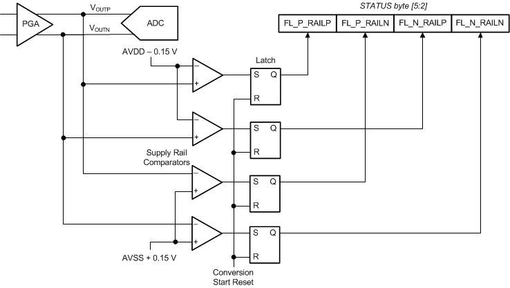 Figure 77. PGA Output Voltage Rail Monitors
Figure 78 shows an example of a PGA output voltage rail monitor overrange event and the respective behavior of the flags. A fault is latched during a conversion cycle. The flags are updated (set or cleared) only at the end of a conversion cycle.
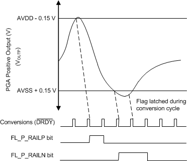 Figure 78. PGA Output Voltage Rail Monitor Timing
9.3.10.4 Reference Monitor
The user can select to continuously monitor the ADC reference inputs for a shorted or missing reference voltage. The reference detection circuit offers two thresholds, the first threshold is 300 mV and the second threshold is
1/3 · (AVDD – AVSS). The reference detection circuit measures the differential reference voltage and sets a flag latched after each conversion in the STATUS byte if the voltage is below the threshold. A reference voltage less than 300 mV can indicate a potential short on the reference inputs or, in case of a ratiometric RTD measurement, a broken wire between the RTD and the reference resistor. A reference voltage between 300 mV and
1/3 · (AVDD – AVSS) can indicate a broken sensor excitation wire in a 3-wire RTD setup.
Additionally, a resistor of 10 MΩ can be connected between the selected REFPx and REFNx inputs. The resistor can be used to detect a floating reference input. With a floating input, the resistor pulls both reference inputs to the same potential so that the reference detection circuit can detect this condition. The pull-together reference resistor is not recommended to be continuously connected to active reference inputs. This resistor lowers the input impedance of the reference inputs and can contribute gain error to the measurement.
The reference detection circuits must be enabled with the FL_REF_EN[1:0] bits of the reference control register (05h). The FL_REF_L0 flag (bit 0 of the STATUS byte) indicates if the reference voltage is lower than 0.3 V. The FL_REF_L1 flag (bit 1 of the STATUS byte) indicates if the reference voltage is lower than
1/3 · (AVDD – AVSS). A diagram of the reference detection circuit is shown in Figure 79. A reference monitor fault is latched at each conversion cycle and the flags in the status register are updated at the falling edge of DRDY.
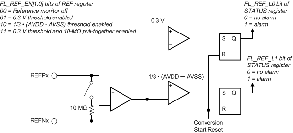 Figure 79. Reference Monitor Block Diagram
9.3.11 General-Purpose Inputs and Outputs (GPIOs)
The ADS114S06 offers four dedicated general-purpose input and output (GPIO) pins, and the ADS114S08 offers four pins (AIN8 to AIN11) that serve a dual purpose as either analog inputs or GPIOs.
Two registers control the function of the GPIO pins. Use the CON[3:0] bits of the GPIO configuration register (11h) to configure a pin as a GPIO pin. The upper four bits (DIR[3:0]) of the GPIO data register (10h) configure the GPIO pin as either an input or an output. The lower four bits (DAT[3:0]) of the GPIO data register contain the input or output GPIO data. If a GPIO pin is configured as an input, the respective DAT[x] bit reads the status of the pin; if a GPIO pin is configured as an output, write the output status to the respective DAT[x] bit. For more information about the use of GPIO pins, see the Configuration Registers section.
Figure 80 shows a diagram of how these functions are combined onto a single pin. Note that when the pin is configured as a GPIO, the corresponding logic is powered from AVDD and AVSS. When the devices are operated with bipolar analog supplies, the GPIO outputs bipolar voltages. Care must be taken to not load the GPIO pins when used as outputs because large currents can cause droop or noise on the analog supplies. GPIO pins use Schmitt triggered inputs, with hysteresis to make the input more resistance to noise; see the Electrical Characteristics table for GPIO thresholds.
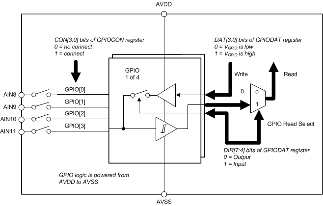 Figure 80. GPIO Block Diagram
For connections of unused GPIO pins, see the Unused Inputs and Outputs section.
9.3.12 Low-Side Power Switch
A low-side power switch with low on-resistance connected between REFN0 and AVSS-SW is integrated in the devices. This power switch can be used to reduce system power consumption in resistive bridge sensor applications by powering down the bridge circuit between conversions. When the PSW bit in the excitation current register 1 (06h) is set to 1, the switch closes. The switch automatically opens when the POWERDOWN command is issued. The switch is opened by setting the PSW bit to 0. By default, the switch is open. Connect AVSS-SW to AVSS.
9.3.13 Cyclic Redundancy Check (CRC)
A cyclic redundancy check (CRC) is enabled by setting the CRC bit to 1 in the system control register (10h). When CRC mode is enabled, the 8-bit CRC is appended to the conversion result. The CRC is calculated for the 16-bit conversion result and the STATUS byte when enabled.
In CRC mode, the checksum byte is the 8-bit remainder of the bitwise exclusive-OR (XOR) of the data bytes by a CRC polynomial. For conversion data, use three data bytes. The CRC is based on the CRC-8-ATM (HEC) polynomial: X8 + X2 + X + 1.
The nine binary coefficients of the polynomial are: 100000111. To calculate the CRC, divide (XOR operation) the data bytes (excluding the CRC) with the polynomial and compare the calculated CRC values to the ADC CRC value. If the values do not match, a data transmission error has occurred. In the event of a data transmission error, read the data again.
The following list shows a general procedure to compute the CRC value:
- Left-shift the initial 16-bit data value (24-bit data when the STATUS byte is enabled) by 8 bits, with zeros padded to the right, creating a new 24-bit data value (the starting data value).
- Align the MSB of the CRC polynomial (100000111) to the left-most, logic-one value of the data.
- Perform an XOR operation on the data value with the aligned CRC polynomial. The XOR operation creates a new, shorter-length value. The bits of the data values that are not in alignment with the CRC polynomial drop down and append to the right of the new XOR result.
- When the XOR result is less than 100000000, the procedure ends, yielding the 8-bit CRC value. Otherwise, continue with the XOR operation shown in step 2, using the current data value. The number of loop iterations depends on the value of the initial data.
9.3.14 Calibration
The ADC incorporates offset and gain calibration commands, as well as user-offset and full-scale (gain) calibration registers to calibrate the ADC. The ADC calibration registers are 16 bits wide. Use calibration to correct internal ADC errors or overall system errors. Calibrate by sending calibration commands to the ADC, or by direct user calibration. In user calibration, the user calculates and writes the correction values to the calibration registers. The ADC performs self or system-offset calibration, or a system gain calibration. Perform offset calibration before system gain calibration. After power-on, wait for the power supplies and reference voltage to fully settle before calibrating.
As shown in Figure 81, the value of the offset calibration register is subtracted from the filter output and then multiplied by the full-scale register value divided by 4000h. The data are then clipped to a 16-bit value to provide the final output.
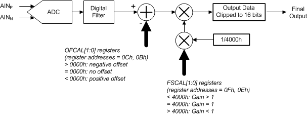 Figure 81. ADC Calibration Block Diagram
Calibration commands cannot be used when the device is in standby mode (when the START/SYNC pin is low, or when the STOP command is issued).
9.3.14.1 Offset Calibration
The offset calibration word is 16 bits, consisting of two 8-bit registers, as shown in the two registers starting with offset calibration register 1. The offset value is twos complement format with a maximum positive value equal to 7FFFh, and a maximum negative value equal to 8000h. This value is subtracted from each output reading as an offset correction. A register value equal to 0000h has no offset correction. If global chop mode is enabled, the offset calibration register is disabled. Table 21 shows example settings of the offset register.
Table 21. Offset Calibration Register Values
| OFC REGISTER VALUE | OFFSET CALIBRATED OUTPUT CODE(1) |
|---|---|
| 0001h | FFFFh |
| 0000h | 0000h |
| FFFFh | 0001h |
The user can select how many samples (1, 4, 8, or 16) to average for self or system offset calibration using the CAL_SAMP[1:0] bits in the system control register (09h). Fewer readings shorten the calibration time but also provide less accuracy. Averaging more readings takes longer but yields a more accurate calibration result by reducing the noise level.
Two commands can be used to perform offset calibration. SFOCAL is a self offset calibration that internally sets the input to mid-scale using the SYS_MON[2:0] = 001 setting and takes a measurement of the offset. SYOCAL is a system offset calibration where the user must input a null voltage to calibrate the system offset. After either command is issued, the OFC register is updated.
After an offset calibration is performed, the device starts a new conversion and DRDY falls to indicate a new conversion has completed.
9.3.14.2 Gain Calibration
The full-scale (gain) calibration word is 16 bits consisting of two 8-bit registers, as shown in the two registers starting with gain calibration register 1. The gain calibration value is straight binary, normalized to a unity-gain correction factor at a register value equal to 4000h. Table 22 shows register values for selected gain factors. Do not exceed the PGA input range limits during gain calibration.
Table 22. Gain Calibration Register Values
| FSC REGISTER VALUE | GAIN FACTOR |
|---|---|
| 4333h | 1.05 |
| 4000h | 1.00 |
| 3CCCh | 0.95 |
All gains of the ADS114S0x are factory trimmed to meet the gain error specified in the Electrical Characteristics table at TA = 25°C. When the gain drift of the devices over temperature is very low, there is typically no need for self gain calibration.
The SYGCAL command initiates a system gain calibration, where the user sets the input to full-scale to remove gain error. After the SYGCAL is issued, the FSC register is updated. As with the offset calibration, the CAL_SAMP[1:0] bits determine the number of samples used for a gain calibration.
As with an offset calibration, the device starts a new conversion after a gain calibration and DRDY falls to indicate a new conversion has completed.
9.4 Device Functional Modes
The device operates in three different modes: power-down mode, standby mode, and conversion mode. Figure 82 shows a flow chart of the different operating modes and how the device transitions from one mode to another.
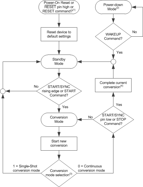
9.4.1 Reset
The ADS114S0x is reset in one of three ways:
- Power-on reset
- RESET pin
- RESET command
When a reset occurs, the configuration registers reset to default values and the device enters standby mode. The device then waits for the rising edge of the START/SYNC pin or a START command to enter conversion mode. Note that if the device had been using an external clock, the reset sets the device to use the internal oscillator as a default configuration. See the Timing Characteristics section for reset timing information.
9.4.1.1 Power-On Reset
The ADS114S0x incorporates a power-on reset circuit that holds the device in reset until all supplies reach approximately 1.65 V. The power-on reset also ensures that the device starts operating in a known state in case a brown-out event occurs, when the supplies have dipped below the minimum operating voltages. When the device completes a POR sequence, the FL_POR flag in the status register is set high to indicate that a POR has occurred.
Begin communications with the device 2.2 ms after the power supplies reach minimum operating voltages. The only exception is polling the status register for the RDY bit. If the user polls the RDY bit, then use an SCLK rate of half the maximum-specified SCLK rate to get a proper reading when the device is making internal configurations. This 2.2-ms POR time is required for the internal oscillator to start up and the device to properly set internal configurations. After the internal configurations are set, the device sets the RDY bit in the device status register (01h). When this bit is set to 0, user configurations can be programmed into the device. Figure 83 shows the power-on reset timing sequence for the device.
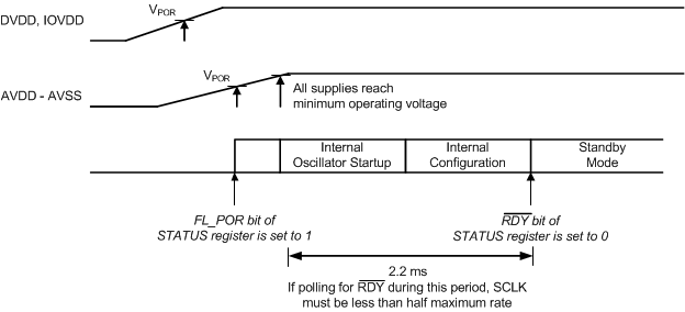 Figure 83. Power-On Reset Timing Sequence
9.4.1.2 RESET Pin
Reset the ADC by taking the RESET pin low for a minimum of 4 · tCLK· cycles, and then returning the pin high. After the rising edge of the RESET pin, a delay time of td(RSSC) is required before sending the first serial interface command or starting a conversion. See the Timing Characteristics section for reset timing information.
9.4.1.3 Reset by Command
Reset the ADC by using the RESET command (06h or 07h). The command is decoded on the seventh SCLK falling edge. After sending the RESET command, a delay time of td(RSSC) is required before sending the first serial interface command or starting a conversion. See the Timing Characteristics section for reset timing information.
9.4.2 Power-Down Mode
Power-down mode is entered by sending the POWERDOWN command. In this mode, all analog and digital circuitry is powered down for lowest power consumption regardless of the register settings. Only the internal voltage reference can be configured to stay on during power-down mode in case a faster start-up time is required. All register values retain the current settings during power-down mode. The configuration registers can be read and written in power-down mode. A WAKEUP command must be issued in order to exit power-down mode and to enter standby mode.
When the POWERDOWN command is issued, the device enters power-down mode 2 · tCLK after the seventh SCLK falling edge of the command. For lowest power consumption (on DVDD and IOVDD), stop the external clock when in power-down mode. The device does not gate the external clock when in power-down mode. Selecting the internal oscillator before sending the POWERDOWN command is recommended.
To release the device from POWERDOWN, issue the WAKEUP command to enter standby mode. The device then waits for the rising edge of the START/SYNC pin or a START command to go into conversion mode.
When in power-down mode, the device responds to the RREG, RDATA, and WAKEUP commands. The WREG and RESET commands can also be sent, but are ignored until a WAKEUP command is sent and the internal oscillator resumes operation.
9.4.3 Standby Mode
The device powers up in standby mode and automatically enters this mode whenever there is no ongoing conversion. When the STOP command is sent (or the START/SYNC pin is taken low) in continuous conversion mode, or when a conversion completes in single-shot conversion mode, the device enters standby mode.
Standby mode offers several different options and features to lower the power consumption:
- The PGA can be powered down by setting PGA_EN[1:0] to 00 in the gain setting register (03h).
- The internal voltage reference can be powered down by setting REFCON[1:0] to 00 in the reference control register (05h). This setting also turns off the IDACs.
- The digital filter is held in reset state.
- The clock to the modulator and digital core is gated to decrease dynamic switching losses.
If powered down in standby mode, the PGA and internal reference can require extra time to power up. Extra delay may be required between power up of the PGA or the internal reference, and the start of conversions. In particular, the reference power up time is dependent on the capacitance between REFOUT and REFCOM.
Calibration commands are not decoded when the device is in standby mode.
9.4.4 Conversion Modes
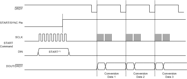
The ADS114S0x offers two conversion modes: continuous conversion and single-shot conversion mode. Continuous-conversion mode converts indefinitely until stopped by the user. Single-shot conversion mode performs one conversion after the START/SYNC pin is taken high or after the START command is sent. Use the MODE bit in the data rate register (04h) to program the conversion mode. Figure 84 shows how the START/SYNC pin and the START command are used to control ADC conversions.
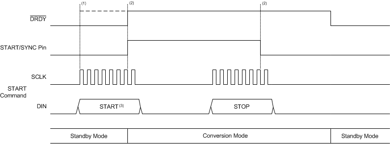
ADC conversions are controlled by the START/SYNC pin or by serial commands. For the device to start converting in continuous conversion or single-shot conversion mode, a START command must be sent or the START/SYNC pin must be taken high. If using commands to control conversions, keep the START/SYNC pin low to avoid possible contentions between the START/SYNC pin and commands.
Conversions can be synchronized to perform a conversion at a particular time. To synchronize the conversion with the START/SYNC pin, take the pin low. The rising edge of the START/SYNC pin starts a new conversion. Similarly, a conversion can be synchronized using the START command. If the device is in standby mode, issue a START command. If the device is in conversion mode, issue a STOP command followed by a START command. The STOP and START commands can be consecutive. A new conversion starts on the seventh SCLK falling edge of the START command.
9.4.4.1 Continuous Conversion Mode
The device is configured for continuous conversion mode by setting the MODE bit to 0 in the data rate register (04h). A START command must be sent or the START/SYNC pin must be taken high for the device to start converting continuously. When controlling the device with commands, hold the START/SYNC pin low. Taking the START/SYNC pin low or sending the STOP command stops the device from converting after the currently ongoing conversion completes, indicated by the falling edge of DRDY. The device enters standby mode thereafter.
For information on the exact timing of single-shot conversion mode data, see Table 13 and Table 15.
9.4.4.2 Single-Shot Conversion Mode
The device is configured for single-shot conversion mode by setting the MODE bit to 1 in the data rate register (04h). A START command must be sent or the START/SYNC pin must be taken high for the device to start a single conversion. After the conversion completes, the device enters standby mode again. To start a new conversion, the START command must be sent again or the START/SYNC pin must be taken low and then high again.
When the device uses the sinc3 filter, ADC data requires three conversion cycles to settle. When the sinc3 filter is enabled, a single-shot conversion suppresses the first two ADC conversions and provides the third conversion as the output data so that the user receives settled data. Because three conversions are required for settled data, the conversion time in single-shot conversion mode is approximately three times the normal data period. When the device uses the low-latency filter, the ADC data settles in a single conversion. In single-shot conversion mode with the low-latency filter, the data period is closer to the normal data period.
For information on the exact timing of single-shot conversion mode data, see Table 13 and Table 15.
9.4.4.3 Programmable Conversion Delay
When a new conversion is started, the ADC provides a delay before the actual start of the conversion. This timed delay is provided to allow for the integrated analog anti-alias filter to settle. In some cases more delay is required to allow for external settling effects. The delay time can be configured to automatically delay the start of a conversion after a START command is sent, the START/SYNC pin is taken high, or a WREG command is sent to change any configuration register from address 03h to 07h is issued (as described in the WREG section). The programmable conversion delay is intended to accommodate the analog settling time on the inputs (for example, when changing a multiplexer channel). Use the DELAY[2:0] bits in the gain setting register (03h) to program a delay time ranging from 1 · tMOD to 4096 · tMOD (where tMOD = 16 · tCLK). The default programmable conversion delay setting is 14 · tMOD.
9.5 Programming
9.5.1 Serial Interface
The ADC has an SPI-compatible, bidirectional serial interface that is used to read the conversion data as well as to configure and control the ADC. Only SPI mode 1 (CPOL = 0, CPHA = 1) is supported. The serial interface consists of five control lines: CS, SCLK, DIN, DOUT/DRDY, and DRDY but can be used with only four or even three control signals. If the ADS114S08 or ADS114S06 is the only device connected to the SPI bus, then the CS input can be tied low so that only SCLK, DIN, and DOUT/DRDY are required to communicate with the device.
9.5.1.1 Chip Select (CS)
The CS pin is an active low input that enables the ADC serial interface for communication and is useful when multiple devices share the same serial bus. CS must be low during the entire data transaction. When CS is high, the serial interface is reset, SCLK input activity is ignored (blocking input commands), and the DOUT/DRDY output enters a high-impedance state. ADC conversions are not affected by the state of CS. In situations where multiple devices are present on the bus, the dedicated DRDY pin can provide an uninterrupted monitor of the conversion status and is not affected by CS. If the serial bus is not shared with another peripheral, CS can be tied to DGND to permanently enable the ADC interface and DOUT/DRDY can be used to indicate conversion status. These changes reduce the serial interface from five I/Os to three I/Os.
9.5.1.2 Serial Clock (SCLK)
The serial interface clock is a noise-filtered, Schmidt-triggered input used to clock data into and out of the ADC. Input data to the ADC are latched on the falling SCLK edge and output data from the ADC are updated on the rising SCLK edge. Return SCLK low after the data sequence is complete. Even though the SCLK input has hysteresis, keep SCLK as clean as possible to prevent unintentional SCLK transitions. Avoid ringing and voltage overshoot on the SCLK input. Place a series termination resistor at the SCLK drive pin to help reduce ringing.
9.5.1.3 Serial Data Input (DIN)
The serial data input pin (DIN) is used with SCLK to send data (commands and register data) to the device. The device latches data on DIN on the SCLK falling edge. The device never drives the DIN pin. During data readback, when no command is intended, keep DIN low.
9.5.1.4 Serial Data Output and Data Ready (DOUT/DRDY)
The DOUT/DRDY pin is a dual-function output. The pin functions as the digital data output and the ADC data-ready indication.
First, this pin is used with SCLK to read conversion and register data from the device. Conversion or register data are shifted out on DOUT/DRDY on the SCLK rising edge. DOUT/DRDY goes to a high-impedance state when CS is high.
Second, the DOUT/DRDY pin indicates availability of new conversion data. DOUT/DRDY transitions low at the same time that the DRDY pin goes low to indicate new conversion data are available. Both signals can be used to detect if new data are ready. However, because DOUT/DRDY is disabled when CS is high, use the dedicated DRDY pin when monitoring conversions on multiple devices on the SPI bus.
9.5.1.5 Data Ready (DRDY)
The DRDY pin is an output that transitions low to indicate when conversion data are ready for retrieval. Initially, DRDY is high at power-on. When converting, the state of DRDY depends on whether the conversion data are retrieved or not. In continuous conversion mode after DRDY goes low, DRDY is driven high on the first SCLK rising edge. If data are not read, DRDY remains low and then pulses high 24 · tCLK before the next DRDY falling edge. The data must be retrieved before the next DRDY update, otherwise the data are overwritten by new data and any previous data are lost. Figure 85 shows the DRDY operation without data retrieval. Figure 86 shows the DRDY operation with data retrieval after each conversion completes.

9.5.1.6 Timeout
The ADS114S0x offers a serial interface timeout feature that is used to recover communication when a serial interface transmission is interrupted. This feature is especially useful in applications where CS is permanently tied low and is not used to frame a communication sequence. The SPI interface resets when no valid 8 bits are received within 215 · tCLK. The timeout feature is enabled by setting the TIMEOUT bit to 1 in the system control register (09h).
9.5.2 Data Format
The devices provide 16 bits of data in binary twos complement format. The size of one code (LSB) is calculated using Equation 11.
A positive full-scale input [VIN ≥ (+FS – 1 LSB) = (VREF / Gain – 1 LSB)] produces an output code of 7FFFh and a negative full-scale input (VIN ≤ –FS = –VREF / Gain) produces an output code of 8000h. The output clips at these codes for signals that exceed full-scale.
Table 23 summarizes the ideal output codes for different input signals.
Table 23. Ideal Output Code vs Input Signal
| INPUT SIGNAL, VIN = VAINP – VAINN |
IDEAL OUTPUT CODE(1) |
|---|---|
| ≥ FS (215 – 1) / 215 | 7FFFh |
| FS / 215 | 0001h |
| 0 | 0000h |
| –FS / 215 | FFFFh |
| ≤ –FS | 8000h |
Mapping of the analog input signal to the output codes is shown in Figure 87.
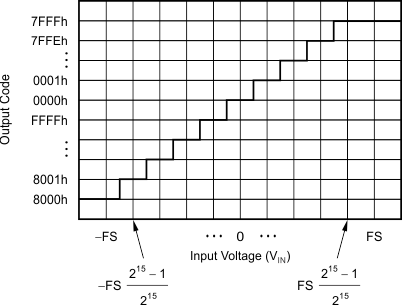 Figure 87. Code Transition Diagram
9.5.3 Commands
Commands are used to control the ADC, access the configuration registers, and retrieve data. Many of the commands are stand-alone (that is, single-byte). The register write and register read commands, however, are multibyte, consisting of two command bytes plus the register data byte or bytes. The commands are listed in Table 24.
Table 24. Command Definitions
| COMMAND | DESCRIPTION | FIRST COMMAND BYTE |
SECOND COMMAND BYTE |
|---|---|---|---|
| Control Commands | |||
| NOP | No operation | 0000 0000 (00h) | — |
| WAKEUP | Wake-up from power-down mode | 0000 001x (02h, 03h)(1) | — |
| POWERDOWN | Enter power-down mode | 0000 010x (04h, 05h)(1) | — |
| RESET | Reset the device | 0000 011x (06h, 07h)(1) | — |
| START | Start conversions | 0000 100x (08h, 09h)(1) | — |
| STOP | Stop conversions | 0000 101x (0Ah, 0Bh)(1) | — |
| Calibration Commands | |||
| SYOCAL | System offset calibration | 0001 0110 (16h) | — |
| SYGCAL | System gain calibration | 0001 0111 (17h) | — |
| SFOCAL | Self offset calibration | 0001 1001 (19h) | — |
| Data Read Command | |||
| RDATA | Read data by command | 0001 001x (12h / 13h)(1) | — |
| Register Read and Write Commands | |||
| RREG | Read nnnnn registers starting at address rrrrr | 001r rrrr(2) | 000n nnnn(3) |
| WREG | Write nnnnn registers starting at address rrrrr | 010r rrrr(2) | 000n nnnn(3) |
Commands can be sent at any time, either during a conversion or when conversions are stopped. However, if register read or write commands are in progress when conversion data are ready, the ADC blocks loading of conversion data to the output shift register. The CS input pin can be taken high between commands; or held low between consecutive commands. CS must stay low for the entire command sequence. Complete the command, or terminate the command before completion by taking CS high. Only send the commands that are listed in Table 24.
9.5.3.1 NOP
NOP is a no-operation command. The NOP command is used to clock out data without clocking in a command.
9.5.3.2 WAKEUP
Issue the WAKEUP command to exit power-down mode and to place the device into standby mode.
When running off the external clock, the external clock must be running before sending the WAKEUP command, otherwise the command is not decoded.
9.5.3.3 POWERDOWN
Sending the POWERDOWN command aborts a currently ongoing conversion and puts the device into power-down mode. The device goes into power-down mode 2 · tCLK after the seventh SCLK falling edge of the command.
For lowest power consumption on DVDD and IOVDD, stop the external clock when in power-down mode. The device does not gate the external clock. When running off the external clock, provide at a minimum two additional tCLKs after the POWERDOWN command is issued, otherwise the device does not enter power-down mode. Because an external clock can be gated for lower power consumption, selecting the internal oscillator before sending the POWERDOWN command is recommended.
During power-down mode, the only commands that are available are RREG, RDATA, and WAKEUP.
9.5.3.4 RESET
The RESET command resets the digital filter and sets all configuration register values to default settings. A RESET command also puts the device into standby mode. When in standby mode, the device waits for a rising edge on the START/SYNC pin or a START command to resume conversions. After sending the RESET command, a delay time of td(RSSC) is required before sending the first serial interface command or starting a conversion. See the Timing Characteristics section for reset timing information.
Note that if the device had been using an external clock, the reset sets the device to use the internal oscillator as a default configuration.
9.5.3.5 START
When the device is configured for continuous conversion mode, issue the START command for the device to start converting. Every time a conversion completes, the device automatically starts a new conversion until the STOP command is sent.
In single-shot conversion mode, the START command is used to start a single conversion. After the conversion completes, the device enters standby mode.
Tie the START/SYNC pin low when the device is controlled through the START and STOP commands. The START command is not decoded if the START/SYNC pin is high. If the device is already in conversion mode, the command has no effect.
9.5.3.6 STOP
The STOP command is used in continuous conversion mode to stop the device from converting. The current conversion is allowed to complete. After DRDY transitions low, the device enters standby mode. The command has no effect in single-shot conversion mode.
Hold the START/SYNC pin low when the device is controlled through START and STOP commands.
9.5.3.7 SYOCAL
The SYOCAL command initiates a system offset calibration. For a system offset calibration, the inputs must be externally shorted to a voltage within the input range, ideally near the mid-supply voltage of (AVDD + AVSS) / 2. The OFC registers are updated when the command completes. Calibration commands must be issued in conversion mode.
9.5.3.8 SYGCAL
The SYGCAL command initiates the system gain calibration. For a system gain calibration, the input must be externally set to full-scale. The FSC registers are updated after this operation. Calibration commands must be issued in conversion mode.
9.5.3.9 SFOCAL
The SFOCAL command initiates a self offset calibration. The device internally shorts the inputs to mid-supply and performs the calibration. The OFC registers are updated after this operation. Calibration commands must be issued in conversion mode.
9.5.3.10 RDATA
The RDATA command is used to read conversion data from the device at any time without concern of data corruption when the DRDY or DOUT/DRDY signal cannot be monitored. The conversion result is read from a buffer so that a new data conversion does not corrupt the conversion read.
9.5.3.11 RREG
Use the RREG command to read the device register data. Read the register data one register at a time, or read a block of register data. The starting register address can be any register in the register map. The RREG command consists of two bytes. The first byte specifies the starting register address: 001r rrrr, where r rrrr is the starting register address. The second command byte is the number of registers to read (minus 1): 000n nnnn, where n nnnn is the number of registers to read minus 1.
After the read command is sent, the ADC responds with one or more register data bytes, most significant bit first. If the byte count exceeds the last register address, the ADC begins to output zero data. During the register read operation, any conversion data that becomes available is not loaded to the output shift register to avoid data contention. However, the conversion data can be retrieved later by the RDATA command. After the register read command has started, further commands are blocked until one of the following conditions are met:
- The read operation is completed
- The read operation is terminated by taking CS high
- The read operation is terminated by a serial interface timeout
- The ADC is reset by toggling the RESET pin
Figure 88 depicts a two-register read operation example. As shown, the commands required to read data from two registers starting at register REF (address = 05h) are: command byte 1 = 25h and command byte 2 = 01h. Keep DIN low after the two command bytes are sent.

9.5.3.12 WREG
Use the WREG command to write the device register data. The register data are written one register at a time or as a block of register data. The starting register address is any register in the register map.
The WREG command consists of two bytes. The first byte specifies the starting register address: 010r rrrr, where r rrrr is the starting register address The second command byte is the number of registers to write (minus 1): 000n nnnn, where n nnnn is the number of registers to write minus 1. The following byte (or bytes) is the register data, most significant bit first. If the byte count exceeds the last register address, the ADC ignores the data. After the register write command has started, further commands are blocked until one of the following conditions are met:
- The write operation is completed
- The write operation is terminated by taking CS high
- The write operation is terminated by a serial interface timeout
- The ADC is reset by toggling the RESET pin
Figure 89 depicts a two-register write operation example. As shown, the required commands to write data to two registers starting at register REF (address = 05h) are: command byte 1 = 45h and command byte 2 = 01h.

Writing new data to certain configuration registers resets the digital filter and starts a new conversion if a conversion is in progress. Writing to the following registers triggers a new conversion:
- Channel configuration register (02h)
- Gain setting register (03h)
- Data rate register (04h)
- Reference control register (05h), bits [5:0]
- Excitation current register 1 (06h), bits [3:0]
- Excitation current register 2 (07h)
- System control register (09h), bits [7:5]
When the device is configured with WREG, the first data ready indication occurs after the new conversion completes with the new configuration settings. The previous conversion data are cleared at restart; therefore read the previous data before the register write operation. A WREG to the previously mentioned registers only starts a new conversion if the register data are new (differs from the previous register data) and if a conversion is in progress. If the device is in standby mode, the device sets the configuration according to the WREG data, but does not start a conversion until the START/SYNC pin is taken high or a START command is issued.
9.5.4 Reading Data
ADC data are read by two methods: read data direct or read data by command. The ADC writes new conversion data to the output shift register and the internal data-holding register. Data are read either from the output shift register (in direct mode) or read from the data-holding register (in command mode). Reading data from the data-holding register (command mode) does not require synchronizing the start of data readback to DRDY.
9.5.4.1 Read Data Direct
In this method of data retrieval, ADC conversion data are shifted out directly from the output shift register. No command is necessary. Read data direct requires that no serial activity occur from the falling edge of DRDY to the readback, or the data are invalid. The serial interface is full duplex in the read data direct mode; meaning that commands are decoded during the data readback. If no command is intended, keep DIN low during readback. If an input command is sent during readback, the ADC executes the command, and data corruption can result. Synchronize the data readback to DRDY or to DOUT/DRDY to make sure the data are read before the next DRDY update, or the old data are overwritten with new data.
As shown in Figure 90, the ADC data field is 2, 3, or 4 bytes long. The data field consists of an optional STATUS byte, three bytes of conversion data, and an optional CRC byte. After all bytes are read, the data-byte sequence (including the STATUS byte and CRC byte, if selected) is repeated when continued SCLKs are sent. The byte sequence repeats starting with the first byte. In order to help verify error-free communication, read the same data multiple times in each conversion interval or use the optional CRC byte.
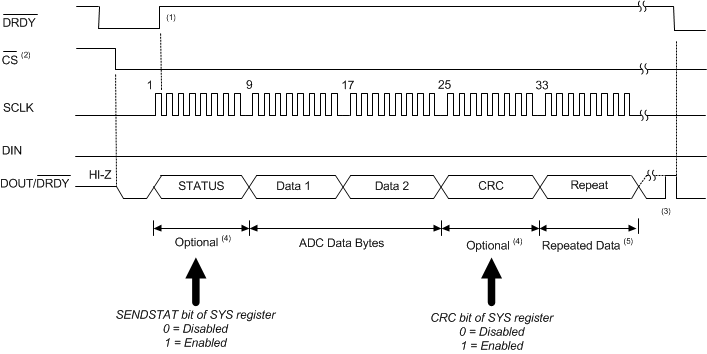
9.5.4.2 Read Data by RDATA Command
When the RDATA command is sent, the data are retrieved from the ADC data-holding register. Read data at any time without the risk of data corruption because the command method does not require synchronizing to DRDY. Polling of DRDY to determine when ADC data are ready can still be used.
Figure 91 shows the read data by command sequence. The output data MSB begins on the first SCLK rising edge after the command. The output data field can be 2, 3, or 4 bytes long. The data field consists of an optional STATUS byte, three bytes of conversion data, and an optional CRC byte. An RDATA command must be sent for each read operation. The ADC does not respond to commands until the read operation is complete, or terminated by taking CS high.
After all bytes are read, the data-byte sequence (including the STATUS byte and CRC byte, if selected) is repeated by continuing SCLK.
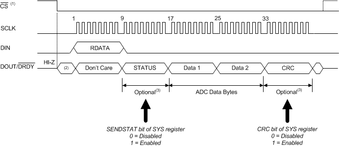
9.5.4.3 Sending Commands When Reading Data
The device serial interface is capable of full-duplex operation when reading conversion data and not using the RDATA command. In full-duplex operation, commands are decoded at the same time that conversion data are read. Commands can be sent on any 8-bit data boundary during a data read operation. When a RREG or RDATA command is recognized, the current data read operation is aborted and the conversion data are corrupted, unless the command is sent when the last byte of the conversion result is retrieved. The device starts to output the requested data on DOUT/DRDY at the first SCLK rising edge after the command byte. To read data without interruption, keep DIN low when clocking out data.
A WREG command can be sent without corrupting an ongoing read operation. Sending a WREG command when reading data minimizes the time between reading the data and setting the device configuration for the next conversion. Figure 92 shows an example for sending a WREG command to write two configuration registers when reading conversion data by using read data direct mode. After the command is clocked in, the device resets the digital filter and starts converting with the new register settings as long as the device is in continuous conversion mode. The digital filter is reset and conversions are restarted after each data byte is received. In this example, the digital filter is reset when the first byte is received, decoding the input multiplexer and again when the PGA is set. The WREG command can be sent on any of the 8-bit boundaries. The example in Figure 92 has the STATUS and CRC bytes disabled.
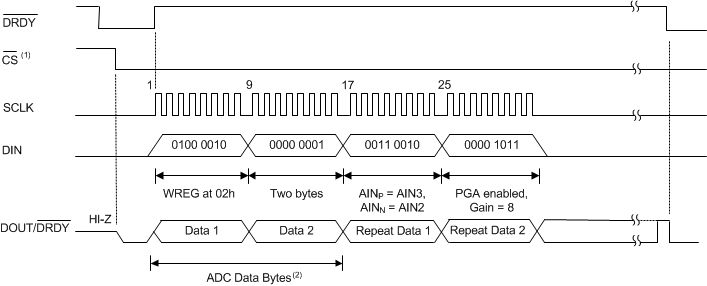
9.5.5 Interfacing with Multiple Devices
When connecting multiple devices to a single SPI bus, SCLK, DIN, and DOUT/DRDY can be safely shared by using a dedicated chip-select (CS) line for each SPI-enabled device. When CS transitions high for the respective device, DOUT/DRDY enters a tri-state mode. Therefore, DOUT/DRDY cannot be used to indicate when new data are available if CS is high. Only the dedicated DRDY pin indicates that new data are available because the DRDY pin is actively driven even when CS is high.
In some cases, the DRDY pin cannot be interfaced to the microcontroller. This scenario can occur if there are insufficient GPIO channels available on the microcontroller or if the serial interface must be galvanically isolated and thus the amount of channels must be limited. In order to evaluate when a new conversion of one of the devices is ready, the microcontroller can periodically drop CS to the respective device and poll the state of the DOUT/DRDY pin.
When CS goes low, the DOUT/DRDY pin immediately drives either high or low. If the DOUT/DRDY line drives low, new data are available. If the DOUT/DRDY line drives high, no new data are available. This procedure requires that DOUT/DRDY is forced high after reading each conversion result and before taking CS high. To make sure DOUT/DRDY is taken high, send a RREG command to read a register where the least significant bit is 1.
Retrieving data using direct read mode requires knowledge of the DRDY falling edge timing to avoid data corruption. Use the RDATA command so that valid data can be retrieved from the device at any time without concern of data corruption by a new data ready.
9.6 Register Map
9.6.1 Configuration Registers
The ADS114S0x register map consists of 18, 8-bit registers. These registers are used to configure and control the device to the desired mode of operation. Access the registers through the serial interface by using the RREG and WREG register commands. After power-on or reset, the registers default to the initial settings, as shown in the Default column of Table 25.
Data can be written as a block to multiple registers using a single WREG command. If data are written as a block, the data of certain registers take effect immediately when data are shifted in. Writing new data to certain registers results in a restart of conversions that are in progress. The registers that result in a conversion restart are discussed in the WREG section.
Table 25. Configuration Register Map
| ADDR | REGISTER | DEFAULT | BIT 7 | BIT 6 | BIT 5 | BIT 4 | BIT 3 | BIT 2 | BIT 1 | BIT 0 |
| 00h | ID | xxh | RESERVED | DEV_ID[2:0] | ||||||
| 01h | STATUS | 80h | FL_POR | RDY | FL_P_RAILP | FL_P_RAILN | FL_N_RAILP | FL_N_RAILN | FL_REF_L1 | FL_REF_L0 |
| 02h | INPMUX | 01h | MUXP[3:0] | MUXN[3:0] | ||||||
| 03h | PGA | 00h | DELAY[2:0] | PGA_EN[1:0] | GAIN[2:0] | |||||
| 04h | DATARATE | 14h | G_CHOP | CLK | MODE | FILTER | DR[3:0] | |||
| 05h | REF | 10h | FL_REF_EN[1:0] | REFP_BUF | REFN_BUF | REFSEL[1:0] | REFCON[1:0] | |||
| 06h | IDACMAG | 00h | FL_RAIL_EN | PSW | 0 | 0 | IMAG[3:0] | |||
| 07h | IDACMUX | FFh | I2MUX[3:0] | I1MUX[3:0] | ||||||
| 08h | VBIAS | 00h | VB_LEVEL | VB_AINC | VB_AIN5 | VB_AIN4 | VB_AIN3 | VB_AIN2 | VB_AIN1 | VB_AIN0 |
| 09h | SYS | 10h | SYS_MON[2:0] | CAL_SAMP[1:0] | TIMEOUT | CRC | SENDSTAT | |||
| 0Ah | RESERVED | 00h | RESERVED | |||||||
| 0Bh | OFCAL0 | 00h | OFC[7:0] | |||||||
| 0Ch | OFCAL1 | 00h | OFC[15:8] | |||||||
| 0Dh | RESERVED | 00h | RESERVED | |||||||
| 0Eh | FSCAL0 | 00h | FSC[7:0] | |||||||
| 0Fh | FSCAL1 | 40h | FSC[15:8] | |||||||
| 10h | GPIODAT | 00h | DIR[3:0] | DAT[3:0] | ||||||
| 11h | GPIOCON | 00h | 0 | 0 | 0 | 0 | CON[3:0] | |||
9.6.1.1 Device ID Register (address = 00h) [reset = xxh]
| 7 | 6 | 5 | 4 | 3 | 2 | 1 | 0 |
| RESERVED | DEV_ID[2:0] | ||||||
| R-xxh | R-xh | ||||||
| LEGEND: R = Read only; -n = value after reset; -x = variable |
Table 26. Device ID (ID) Register Field Descriptions
| Bit | Field | Type | Reset | Description |
|---|---|---|---|---|
| 7:3 | RESERVED | R | xxh | Reserved
Values are subject to change without notice |
| 2:0 | DEV_ID[2:0] | R | xh | Device identifier
Identifies the model of the device. 000 : Reserved001 : Reserved 010 : Reserved 011 : Reserved 100 : ADS114S08 (12 channels, 16 bits) 101 : ADS114S06 (6 channels, 16 bits) 110 : Reserved 111 : Reserved |
9.6.1.2 Device Status Register (address = 01h) [reset = 80h]
| 7 | 6 | 5 | 4 | 3 | 2 | 1 | 0 |
| FL_POR | RDY | FL_P_RAILP | FL_P_RAILN | FL_N_RAILP | FL_N_RAILN | FL_REF_L1 | FL_REF_L0 |
| R/W-1h | R-0h | R-0h | R-0h | R-0h | R-0h | R-0h | R-0h |
| LEGEND: R/W = Read/Write; R = Read only; -n = value after reset |
Table 27. Device Status (STATUS) Register Field Descriptions
| Bit | Field | Type | Reset | Description |
|---|---|---|---|---|
| 7 | FL_POR | R/W | 1h | POR flag
Indicates a power-on reset (POR) event has occurred. 0 : Register has been cleared and no POR event has occurred.1 : POR event occurred and has not been cleared. Flag must be cleared by user register write (default). |
| 6 | RDY | R | 0h | Device ready flag
Indicates the device has started up and is ready for communication. 0 : ADC ready for communication (default)1 : ADC not ready |
| 5 | FL_P_RAILP | R | 0h | Positive PGA output at positive rail flag(1)
Indicates the positive PGA output is within 150 mV of AVDD. 0 : No error (default)1 : PGA positive output within 150 mV of AVDD |
| 4 | FL_P_RAILN | R | 0h | Positive PGA output at negative rail flag(1)
Indicates the positive PGA output is within 150 mV of AVSS. 0 : No error (default)1 : PGA positive output within 150 mV of AVSS |
| 3 | FL_N_RAILP | R | 0h | Negative PGA output at positive rail flag(1)
Indicates the negative PGA output is within 150 mV of AVDD. 0 : No error (default)1 : PGA negative output within 150 mV of AVDD |
| 2 | FL_N_RAILN | R | 0h | Negative PGA output at negative rail flag(1)
Indicates the negative PGA output is within 150 mV of AVSS. 0 : No error (default)1 : PGA negative output within 150 mV of AVSS |
| 1 | FL_REF_L1 | R | 0h | Reference voltage monitor flag, level 1(2)
Indicates the external reference voltage is lower than 1/3 of the analog supply voltage. Can be used to detect an open-excitation lead in a 3-wire RTD application. 0 : Differential reference voltage ≥ 1/3 · (AVDD – AVSS) (default)1 : Differential reference voltage < 1/3 · (AVDD – AVSS) |
| 0 | FL_REF_L0 | R | 0h | Reference voltage monitor flag, level 0(2)
Indicates the external reference voltage is lower than 0.3 V. Can be used to indicate a missing or floating external reference voltage. 0 : Differential reference voltage ≥ 0.3 V (default)1 : Differential reference voltage < 0.3 V |
9.6.1.3 Input Multiplexer Register (address = 02h) [reset = 01h]
| 7 | 6 | 5 | 4 | 3 | 2 | 1 | 0 |
| MUXP[3:0] | MUXN[3:0] | ||||||
| R/W-0h | R/W-1h | ||||||
| LEGEND: R/W = Read/Write; -n = value after reset |
Table 28. Input Multiplexer (INPMUX) Register Field Descriptions
| Bit | Field | Type | Reset | Description |
|---|---|---|---|---|
| 7:4 | MUXP[3:0] | R/W | 0h | Positive ADC input selection
Selects the ADC positive input channel. 0000 : AIN0 (default)0001 : AIN1 0010 : AIN2 0011 : AIN3 0100 : AIN4 0101 : AIN5 0110 : AIN6 (ADS114S08 only) 0111 : AIN7 (ADS114S08 only) 1000 : AIN8 (ADS114S08 only) 1001 : AIN9 (ADS114S08 only) 1010 : AIN10 (ADS114S08 only) 1011 : AIN11 (ADS114S08 only) 1100 : AINCOM 1101 : Reserved 1110 : Reserved 1111 : Reserved |
| 3:0 | MUXN[3:0] | R/W | 1h | Negative ADC input selection
Selects the ADC negative input channel. 0000 : AIN00001 : AIN1 (default) 0010 : AIN2 0011 : AIN3 0100 : AIN4 0101 : AIN5 0110 : AIN6 (ADS114S08 only) 0111 : AIN7 (ADS114S08 only) 1000 : AIN8 (ADS114S08 only) 1001 : AIN9 (ADS114S08 only) 1010 : AIN10 (ADS114S08 only) 1011 : AIN11 (ADS114S08 only) 1100 : AINCOM 1101 : Reserved 1110 : Reserved 1111 : Reserved |
9.6.1.4 Gain Setting Register (address = 03h) [reset = 00h]
| 7 | 6 | 5 | 4 | 3 | 2 | 1 | 0 |
| DELAY[2:0] | PGA_EN[1:0] | GAIN[2:0] | |||||
| R/W-0h | R/W-0h | R/W-0h | |||||
| LEGEND: R/W = Read/Write; -n = value after reset |
Table 29. Gain Setting (PGA) Register Field Descriptions
| Bit | Field | Type | Reset | Description |
|---|---|---|---|---|
| 7:5 | DELAY[2:0] | R/W | 0h | Programmable conversion delay selection
Sets the programmable conversion delay time for the first conversion after a WREG when a configuration change resets of the digital filter and triggers a new conversion(1). 000 : 14 · tMOD (default)001 : 25 · tMOD 010 : 64 · tMOD 011 : 256 · tMOD 100 : 1024 · tMOD 101 : 2048 · tMOD 110 : 4096 · tMOD 111 : 1 · tMOD |
| 4:3 | PGA_EN[1:0] | R/W | 0h | PGA enable
Enables or bypasses the PGA. 00 : PGA is powered down and bypassed. Enables single-ended measurements with unipolar supply (Set gain = 1(2)) (default)01 : PGA enabled (gain = 1 to 128) 10 : Reserved 11 : Reserved |
| 2:0 | GAIN[2:0] | R/W | 0h | PGA gain selection
Configures the PGA gain. 000 : 1 (default)001 : 2 010 : 4 011 : 8 100 : 16 101 : 32 110 : 64 111 : 128 |
9.6.1.5 Data Rate Register (address = 04h) [reset = 14h]
| 7 | 6 | 5 | 4 | 3 | 2 | 1 | 0 |
| G_CHOP | CLK | MODE | FILTER | DR[3:0] | |||
| R/W-0h | R/W-0h | R/W-0h | R/W-1h | R/W-4h | |||
| LEGEND: R/W = Read/Write; R = Read only; -n = value after reset |
Table 30. Data Rate (DATARATE) Register Field Descriptions
| Bit | Field | Type | Reset | Description |
|---|---|---|---|---|
| 7 | G_CHOP | R/W | 0h | Global chop enable
Enables the global chop function. When enabled, the device automatically swaps the inputs and takes the average of two consecutive readings to cancel the offset voltage. 0 : Disabled (default)1 : Enabled |
| 6 | CLK | R/W | 0h | Clock source selection
Configures the clock source to use either the internal oscillator or an external clock. 0 : Internal 4.096-MHz oscillator (default)1 : External clock |
| 5 | MODE | R/W | 0h | Conversion mode selection
Configures the ADC for either continuous conversion or single-shot conversion mode. 0 : Continuous conversion mode (default)1 : Single-shot conversion mode |
| 4 | FILTER | R/W | 1h | Digital filter selection
Configures the ADC to use either the sinc3 or the low-latency filter. 0 : Sinc3 filter1 : Low-latency filter (default) |
| 3:0 | DR[3:0] | R/W | 4h | Data rate selection
Configures the output data rate(1). 0000 : 2.5 SPS0001 : 5 SPS 0010 : 10 SPS 0011 : 16.6 SPS 0100 : 20 SPS (default) 0101 : 50SPS 0110 : 60 SPS 0111 : 100 SPS 1000 : 200 SPS 1001 : 400 SPS 1010 : 800 SPS 1011 : 1000 SPS 1100 : 2000 SPS 1101 : 4000 SPS 1110 : 4000 SPS 1111 : Reserved |
9.6.1.6 Reference Control Register (address = 05h) [reset = 10h]
| 7 | 6 | 5 | 4 | 3 | 2 | 1 | 0 |
| FL_REF_EN[1:0] | REFP_BUF | REFN_BUF | REFSEL[1:0] | REFCON[1:0] | |||
| R/W-0h | R/W-0h | R/W-1h | R/W-0h | R/W-0h | |||
| LEGEND: R/W = Read/Write; -n = value after reset |
Table 31. Reference Control (REF) Register Field Descriptions
| Bit | Field | Type | Reset | Description |
|---|---|---|---|---|
| 7:6 | FL_REF_EN[1:0] | R/W | 0h | Reference monitor configuration
Enables and configures the reference monitor. 00 : Disabled (default)01 : FL_REF_L0 monitor enabled, threshold 0.3 V 10 : FL_REF_L0 and FL_REF_L1 monitors enabled, thresholds 0.3 V and 1/3 · (AVDD – AVSS) 11 : FL_REF_L0 monitor and 10-MΩ pull-together enabled, threshold 0.3 V |
| 5 | REFP_BUF | R/W | 0h | Positive reference buffer bypass
Disables the positive reference buffer. Recommended when V(REFPx) is close to AVDD. 0 : Enabled (default)1 : Disabled |
| 4 | REFN_BUF | R/W | 1h | Negative reference buffer bypass
Disables the negative reference buffer. Recommended when V(REFNx) is close to AVSS. 0 : Enabled1 : Disabled (default) |
| 3:2 | REFSEL[1:0] | R/W | 0h | Reference input selection
Selects the reference input source for the ADC. 00 : REFP0, REFN0 (default)01 : REFP1, REFN1 10 : Internal 2.5-V reference(1) 11 : Reserved |
| 1:0 | REFCON[1:0] | R/W | 0h | Internal voltage reference configuration(2)
Configures the behavior of the internal voltage reference. 00 : Internal reference off (default)01 : Internal reference on, but powers down in power-down mode 10 : Internal reference is always on, even in power-down mode 11 : Reserved |
9.6.1.7 Excitation Current Register 1 (address = 06h) [reset = 00h]
| 7 | 6 | 5 | 4 | 3 | 2 | 1 | 0 |
| FL_RAIL_EN | PSW | 0 | 0 | IMAG[3:0] | |||
| R/W-0h | R/W-0h | R-0h | R-0h | R/W-0h | |||
| LEGEND: R/W = Read/Write; R = Read only; -n = value after reset |
Table 32. Excitation Current Register 1 (IDACMAG) Register Field Descriptions
| Bit | Field | Type | Reset | Description |
|---|---|---|---|---|
| 7 | FL_RAIL_EN | R/W | 0h | PGA output rail flag enable
Enables the PGA output voltage rail monitor circuit. 0 : Disabled (default)1 : Enabled |
| 6 | PSW | R/W | 0h | Low-side power switch
Controls the low-side power switch. The low-side power switch opens automatically in power-down mode. 0 : Open (default)1 : Closed |
| 5:4 | RESERVED | R | 0h | Reserved
Always write 0h |
| 3:0 | IMAG[3:0] | R/W | 0h | IDAC magnitude selection
Selects the value of the excitation current sources. Sets IDAC1 and IDAC2 to the same value. 0000 : Off (default)0001 : 10 µA 0010 : 50 µA 0011 : 100 µA 0100 : 250 µA 0101 : 500 µA 0110 : 750 µA 0111 : 1000 µA 1000 : 1500 µA 1001 : 2000 µA 1010 - 1111 : Off |
9.6.1.8 Excitation Current Register 2 (address = 07h) [reset = FFh]
| 7 | 6 | 5 | 4 | 3 | 2 | 1 | 0 |
| I2MUX[3:0] | I1MUX[3:0] | ||||||
| R/W-Fh | R/W-Fh | ||||||
| LEGEND: R/W = Read/Write; -n = value after reset |
Table 33. Excitation Current Register 2 (IDACMUX) Register Field Descriptions
| Bit | Field | Type | Reset | Description |
|---|---|---|---|---|
| 7:4 | I2MUX[3:0] | R/W | Fh | IDAC2 output channel selection
Selects the output channel for IDAC2. 0000 : AIN00001 : AIN1 0010 : AIN2 0011 : AIN3 0100 : AIN4 0101 : AIN5 0110 : AIN6 (ADS114S08), REFP1 (ADS114S06) 0111 : AIN7 (ADS114S08), REFN1 (ADS114S06) 1000 : AIN8 (ADS114S08 only) 1001 : AIN9 (ADS114S08 only) 1010 : AIN10 (ADS114S08 only) 1011 : AIN11 (ADS114S08 only) 1100 : AINCOM 1101 - 1111 : Disconnected (default) |
| 3:0 | I1MUX[3:0] | R/W | Fh | IDAC1 output channel selection
Selects the output channel for IDAC1. 0000 : AIN00001 : AIN1 0010 : AIN2 0011 : AIN3 0100 : AIN4 0101 : AIN5 0110 : AIN6 (ADS114S08 only), REFP1 (ADS114S06) 0111 : AIN7 (ADS114S08 only), REFN1 (ADS114S06) 1000 : AIN8 (ADS114S08 only) 1001 : AIN9 (ADS114S08 only) 1010 : AIN10 (ADS114S08 only) 1011 : AIN11 (ADS114S08 only) 1100 : AINCOM 1101 - 1111 : Disconnected (default) |
9.6.1.9 Sensor Biasing Register (address = 08h) [reset = 00h]
| 7 | 6 | 5 | 4 | 3 | 2 | 1 | 0 |
| VB_LEVEL | VB_AINC | VB_AIN5 | VB_AIN4 | VB_AIN3 | VB_AIN2 | VB_AIN1 | VB_AIN0 |
| R/W-0h | R/W-0h | R/W-0h | R/W-0h | R/W-0h | R/W-0h | R/W-0h | R/W-0h |
| LEGEND: R/W = Read/Write; -n = value after reset |
Table 34. Sensor Biasing (VBIAS) Register Field Descriptions
| Bit | Field | Type | Reset | Description |
|---|---|---|---|---|
| 7 | VB_LEVEL | R/W | 0h | VBIAS level selection
Sets the VBIAS output voltage level. VBIAS is disabled when not connected to any input. 0 : (AVDD + AVSS) / 2 (default)1 : (AVDD + AVSS) / 12 |
| 6 | VB_AINC | R/W | 0h | AINCOM VBIAS selection(1)
Enables VBIAS on the AINCOM pin. 0 : VBIAS disconnected from AINCOM (default)1 : VBIAS connected to AINCOM |
| 5 | VB_AIN5 | R/W | 0h | AIN5 VBIAS selection(1)
Enables VBIAS on the AIN5 pin. 0 : VBIAS disconnected from AIN5 (default)1 : VBIAS connected to AIN5 |
| 4 | VB_AIN4 | R/W | 0h | AIN4 VBIAS selection(1)
Enables VBIAS on the AIN4 pin. 0 : VBIAS disconnected from AIN4 (default)1 : VBIAS connected to AIN4 |
| 3 | VB_AIN3 | R/W | 0h | AIN3 VBIAS selection(1)
Enables VBIAS on the AIN3 pin. 0 : VBIAS disconnected from AIN3 (default)1 : VBIAS connected to AIN3 |
| 2 | VB_AIN2 | R/W | 0h | AIN2 VBIAS selection(1)
Enables VBIAS on the AIN2 pin. 0 : VBIAS disconnected from AIN2 (default)1 : VBIAS connected to AIN2 |
| 1 | VB_AIN1 | R/W | 0h | AIN1 VBIAS selection(1)
Enables VBIAS on the AIN1 pin. 0 : VBIAS disconnected from AIN1 (default)1 : VBIAS connected to AIN1 |
| 0 | VB_AIN0 | R/W | 0h | AIN0 VBIAS selection(1)
Enables VBIAS on the AIN0 pin. 0 : VBIAS disconnected from AIN0 (default)1 : VBIAS connected to AIN0 |
9.6.1.10 System Control Register (address = 09h) [reset = 10h]
| 7 | 6 | 5 | 4 | 3 | 2 | 1 | 0 |
| SYS_MON[2:0] | CAL_SAMP[1:0] | TIMEOUT | CRC | SENDSTAT | |||
| R/W-0h | R/W-2h | R/W-0h | R/W-0h | R/W-0h | |||
| LEGEND: R/W = Read/Write; -n = value after reset |
Table 35. System Control (SYS) Register Field Descriptions
| Bit | Field | Type | Reset | Description |
|---|---|---|---|---|
| 7:5 | SYS_MON[2:0] | R/W | 0h | System monitor configuration(1)
Enables a set of system monitor measurements using the ADC. 000 : Disabled (default)001 : PGA inputs shorted to (AVDD + AVSS) / 2 and disconnected from AINx and the multiplexer; gain set by user 010 : Internal temperature sensor measurement; PGA must be enabled (PGA_EN[1:0] = 01); gain set by user(2) 011 : (AVDD – AVSS) / 4 measurement; gain set to 1(3) 100 : DVDD / 4 measurement; gain set to 1(3) 101 : Burn-out current sources enabled, 0.2-µA setting 110 : Burn-out current sources enabled, 1-µA setting 111 : Burn-out current sources enabled, 10-µA setting |
| 4:3 | CAL_SAMP[1:0] | R/W | 2h | Calibration sample size selection
Configures the number of samples averaged for self and system offset and system gain calibration. 00 : 1 sample01 : 4 samples 10 : 8 samples (default) 11 : 16 samples |
| 2 | TIMEOUT | R/W | 0h | SPI timeout enable
Enables the SPI timeout function. 0 : Disabled (default) 1 : Enabled |
| 1 | CRC | R/W | 0h | CRC enable
Enables the CRC byte appended to the conversion result. When enabled, CRC is calculated across the 16-bit conversion result (plus the STATUS byte if enabled). 0 : Disabled (default) 1 : Enabled |
| 0 | SENDSTAT | R/W | 0h | STATUS byte enable
Enables the STATUS byte prepended to the conversion result. 0 : Disabled (default)1 : Enabled |
9.6.1.11 Reserved Register (address = 0Ah) [reset = 00h]
| 7 | 6 | 5 | 4 | 3 | 2 | 1 | 0 |
| RESERVED | |||||||
| R-00h | |||||||
| LEGEND: R/W = Read/Write; -n = value after reset |
Table 36. Reserved Register Field Descriptions
| Bit | Field | Type | Reset | Description |
|---|---|---|---|---|
| 7:0 | RESERVED | R | 00h | Reserved
Always write 00h |
9.6.1.12 Offset Calibration Register 1 (address = 0Bh) [reset = 00h]
| 7 | 6 | 5 | 4 | 3 | 2 | 1 | 0 |
| OFC[7:0] | |||||||
| R/W-00h | |||||||
| LEGEND: R/W = Read/Write; -n = value after reset |
Table 37. Offset Calibration Register 1 (OFCAL0) Register Field Descriptions
| Bit | Field | Type | Reset | Description |
|---|---|---|---|---|
| 7:0 | OFC[7:0] | R/W | 00h | Bits [7:0] of the offset calibration value. |
9.6.1.13 Offset Calibration Register 2 (address = 0Ch) [reset = 00h]
| 7 | 6 | 5 | 4 | 3 | 2 | 1 | 0 |
| OFC[15:8] | |||||||
| R/W-00h | |||||||
| LEGEND: R/W = Read/Write; -n = value after reset |
Table 38. Offset Calibration Register 2 (OFCAL1) Register Field Descriptions
| Bit | Field | Type | Reset | Description |
|---|---|---|---|---|
| 7:0 | OFC[15:8] | R/W | 00h | Bits [15:8] of the offset calibration value. |
9.6.1.14 Reserved Register (address = 0Dh) [reset = 00h]
| 7 | 6 | 5 | 4 | 3 | 2 | 1 | 0 |
| RESERVED | |||||||
| R-00h | |||||||
| LEGEND: R/W = Read/Write; -n = value after reset |
Table 39. Reserved Register Field Descriptions
| Bit | Field | Type | Reset | Description |
|---|---|---|---|---|
| 7:0 | RESERVED | R | 00h | Reserved
Always write 00h |
9.6.1.15 Gain Calibration Register 1 (address = 0Eh) [reset = 00h]
| 7 | 6 | 5 | 4 | 3 | 2 | 1 | 0 |
| FSC[7:0] | |||||||
| R/W-00h | |||||||
| LEGEND: R/W = Read/Write; -n = value after reset |
Table 40. Gain Calibration Register 1 (FSCAL0) Field Descriptions
| Bit | Field | Type | Reset | Description |
|---|---|---|---|---|
| 7:0 | FSC[7:0] | R/W | 00h | Bits [7:0] of the gain calibration value. |
9.6.1.16 Gain Calibration Register 2 (address = 0Fh) [reset = 40h]
| 7 | 6 | 5 | 4 | 3 | 2 | 1 | 0 |
| FSC[15:8] | |||||||
| R/W-40h | |||||||
| LEGEND: R/W = Read/Write; -n = value after reset |
Table 41. Gain Calibration Register 2 (FSCAL1) Field Descriptions
| Bit | Field | Type | Reset | Description |
|---|---|---|---|---|
| 7:0 | FSC[15:8] | R/W | 40h | Bits [15:8] of the gain calibration value. |
9.6.1.17 GPIO Data Register (address = 10h) [reset = 00h]
| 7 | 6 | 5 | 4 | 3 | 2 | 1 | 0 |
| DIR[3:0] | DAT[3:0] | ||||||
| R/W-0h | R/W-0h | ||||||
| LEGEND: R/W = Read/Write; -n = value after reset |
Table 42. GPIO Data (GPIODAT) Register Field Descriptions
| Bit | Field | Type | Reset | Description |
|---|---|---|---|---|
| 7:4 | DIR[3:0] | R/W | 0h | GPIO direction
Configures the selected GPIO as an input or output. 0 : GPIO[x] configured as output (default)1 : GPIO[x] configured as input |
| 3:0 | DAT[3:0] | R/W | 0h | GPIO data
Contains the data of the GPIO inputs or outputs. 0 : GPIO[x] is low (default) 1 : GPIO[x] is high |
9.6.1.18 GPIO Configuration Register (address = 11h) [reset = 00h]
| 7 | 6 | 5 | 4 | 3 | 2 | 1 | 0 |
| 0 | 0 | 0 | 0 | CON[3:0] | |||
| R-0h | R-0h | R-0h | R-0h | R/W-0h | |||
| LEGEND: R/W = Read/Write; R = Read only; -n = value after reset |
Table 43. GPIO Configuration (GPIOCON) Register Field Descriptions
| Bit | Field | Type | Reset | Description |
|---|---|---|---|---|
| 7:4 | RESERVED | R | 0h | Reserved
Always write 0h |
| 3:0 | CON[3:0] | R/W | 0h | GPIO pin configuration
Configures the GPIO[x] pin as an analog input or GPIO. CON[x] corresponds to the GPIO[x] pin. 0 : GPIO[x] configured as analog input (default)(1)1 : GPIO[x] configured as GPIO |