JAJSDA5B November 2017 – November 2020 LM5145
PRODUCTION DATA
- 1 特長
- 2 アプリケーション
- 3 概要
- 4 Revision History
- 5 Description (continued)
- 6 Pin Configuration and Functions
- 7 Specifications
-
8 Detailed Description
- 8.1 Overview
- 8.2 Functional Block Diagram
- 8.3
Feature Description
- 8.3.1 Input Range (VIN)
- 8.3.2 Output Voltage Setpoint and Accuracy (FB)
- 8.3.3 High-Voltage Bias Supply Regulator (VCC)
- 8.3.4 Precision Enable (EN/UVLO)
- 8.3.5 Power Good Monitor (PGOOD)
- 8.3.6 Switching Frequency (RT, SYNCIN)
- 8.3.7 Configurable Soft Start (SS/TRK)
- 8.3.8 Voltage-Mode Control (COMP)
- 8.3.9 Gate Drivers (LO, HO)
- 8.3.10 Current Sensing and Overcurrent Protection (ILIM)
- 8.3.11 OCP Duty Cycle Limiter
- 8.4 Device Functional Modes
-
9 Application and Implementation
- 9.1 Application Information
- 9.2
Typical Applications
- 9.2.1 Design 1 – 20-A High-Efficiency Synchronous Buck Regulator for Telecom Power Applications
- 9.2.2 Design 2 – High Density, 12-V, 10-A Rail With LDO Low-Noise Auxiliary Output for RF Power Applications
- 9.2.3 Design 3 – 150-W, Regulated 24-V Rail for Commercial Drone Applications With Output Voltage Tracking Feature
- 9.2.4 Design 4 – Powering a Multicore DSP From a 24-V or 48-V Rail
- 10Power Supply Recommendations
- 11Layout
- 12Device and Documentation Support
- 13Mechanical, Packaging, and Orderable Information
8.3.7.1 Tracking
The SS/TRK pin also doubles as a tracking pin when master-slave power-supply tracking is required. This tracking is achieved by simply dividing down the output voltage of the master with a simple resistor network. Coincident, ratiometric, and offset tracking modes are possible.
If an external voltage source is connected to the SS/TRK pin, the external soft-start capability of the LM5145 is effectively disabled. The regulated output voltage level is reached when the SS/TRACK pin reaches the 0.8-V reference voltage level. It is the responsibility of the system designer to determine if an external soft-start capacitor is required to keep the device from entering current limit during a start-up event. Likewise, the system designer must also be aware of how fast the input supply ramps if the tracking feature is enabled.
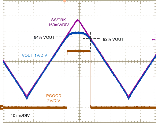
 Figure 8-6 Typical Output Voltage Tracking and PGOOD Waveforms
Figure 8-6 shows a triangular voltage signal directly driving SS/TRK and the corresponding output voltage tracking response. Nominal output voltage here is 5 V, with oscilloscope channel scaling chosen such that the waveforms overlap during tracking. As expected, the PGOOD flag transitions at thresholds of 94% (rising) and 92% (falling) of the nominal output voltage setpoint.
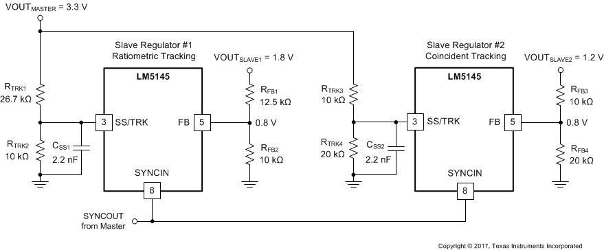
Two practical tracking configurations, ratiometric and coincident, are shown in Figure 8-7. The most common application is coincident tracking, used in core versus I/O voltage tracking in DSP and FPGA implementations. Coincident tracking forces the master and slave channels to have the same output voltage ramp rate until the slave output reaches its regulated setpoint. Conversely, ratiometric tracking sets the output voltage of the slave to a fraction of the output voltage of the master during start-up.
 Figure 8-7 Tracking Implementation With Master, Ratiometric Slave, and Coincident Slave Rails
For coincident tracking, connect the SS/TRK input of the slave regulator to a resistor divider from the output voltage of the master that is the same as the divider used on the FB pin of the slave. In other words, simply select RTRK3 = RFB3 and RTRK4 = RFB4 as shown in Figure 8-7. As the master voltage rises, the slave voltage rises identically (aside from the 80-mV offset from SS/TRK to FB when VFB is below 0.8 V). Eventually, the slave voltage reaches its regulation voltage, at which point the internal reference takes over the regulation while the SS/TRK input continues to 115 mV above FB, and no longer controls the output voltage.
In all cases, to ensure that the output voltage accuracy is not compromised by the SS/TRK voltage being too close to the 0.8-V reference voltage, the final value of the SS/TRK voltage of the slave should be at least 100 mV above FB.