JAJSDH5B December 2008 – July 2017 TPA6132A2
PRODUCTION DATA.
- 1 特長
- 2 アプリケーション
- 3 概要
- 4 改訂履歴
- 5 Pin Configuration and Functions
- 6 Specifications
- 7 Detailed Description
- 8 Application and Implementation
- 9 Power Supply Recommendations
- 10Layout
- 11デバイスおよびドキュメントのサポート
- 12メカニカル、パッケージ、および注文情報
8 Application and Implementation
NOTE
Information in the following applications sections is not part of the TI component specification, and TI does not warrant its accuracy or completeness. TI’s customers are responsible for determining suitability of components for their purposes. Customers should validate and test their design implementation to confirm system functionality.
8.1 Application Information
The TPA6132A2 starts its operation by asserting the EN pin to logic 1. The device enters in shutdown mode when pulling low EN pin. The charge pump generates a negative supply voltage. The charge pump flying capacitor connected between CPP and CPN transfers charge to generate the negative supply voltage. The output voltages are capable of positive and negative voltage swings and are centered close to 0 V, eliminating the need for output capacitors. Input coupling capacitors block any dc bias from the audio source and ensure maximum dynamic range. The device has built-in pop suppression circuitry to completely eliminate pop noise during turn- on, turn-off and enter or exit shutdown mode.
8.2 Typical Applications
8.2.1 Configuration with Differential Input Signals
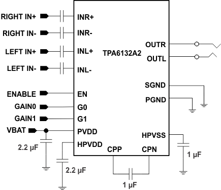
Figure 24 shows a typical application circuit for the TPA6132A2 with a stereo headphone jack output and differential input signals. Also supports charge pump flying capacitor and power supply decoupling capacitors.
 Figure 24. Typical Application Configuration with Differential Input Signals
8.2.1.1 Design Requirements
For this design example, use the parameters shown in Table 2.
Table 2. Design Parameters
| PARAMETERS | VALUES |
|---|---|
| Input voltage range | 2.2 V to 5.3 V |
| Output voltage | 1.1-VRMS |
| Current | 2 mA to 3.2 mA |
8.2.1.2 Detailed Design Procedure
8.2.1.2.1 Input Coupling Capacitors
Input coupling capacitors block any dc bias from the audio source and ensure maximum dynamic range. Input coupling capacitors also minimize TPA6132A2 turn-on pop to an inaudible level.
The input capacitors are in series with TPA6132A2 internal input resistors, creating a high-pass filter. Equation 3 calculates the high-pass filter corner frequency. The input impedance, RIN, is dependent on device gain. Larger input capacitors decrease the corner frequency. See the Operating Characteristics table for input impedance values.

For a given high-pass cutoff frequency, the minimum input coupling capacitor is found as:

Example: Design for a 20 Hz corner frequency with a TPA6132A2 gain of +6 dB. The Operating Characteristics table gives RIN as 13.2 kΩ. Equation 4 shows the input coupling capacitors must be at least 0.6 μF to achieve a 20 Hz high-pass corner frequency. Choose a 0.68 μF standard value capacitor for each TPA6132A2 input (X5R material or better is required for best performance).
Input capacitors can be removed provided the TPA6132A2 inputs are driven differentially with less than ±1 V and the common-mode voltage is within the input common-mode range of the amplifier. Without input capacitors turn-on pop performance may be degraded and should be evaluated in the system.
8.2.1.2.2 Charge Pump Flying Capacitor and HPVSS Capacitor
The TPA6132A2 uses a built-in charge pump to generate a negative voltage supply for the headphone amplifiers. The charge pump flying capacitor connects between CPP and CPN. It transfers charge to generate the negative supply voltage. The HPVSS capacitor must be at least equal in value to the flying capacitor to allow maximum charge transfer. Use low equivalent-series-resistance (ESR) ceramic capacitors (X5R material or better is required for best performance) to maximize charge pump efficiency. Typical values are 1 μF to 2.2 μF for the HPVSS and flying capacitors. Although values down to 0.47 μF can be used, total harmonic distortion (THD) will increase.
8.2.1.3 Application Curves
 Figure 25. Start-Up Time
 Figure 26. Shutdown
8.2.2 Configuration with Single-Ended Input Signals
Figure 27 shows a typical application circuit for the TPA6132A2 with a stereo headphone jack output and single-ended input signals. Also supports charge pump flying capacitor and power supply decoupling capacitors.
 Figure 27. Typical Application Configuration with Single-Ended Input Signals
8.2.2.1 Design Requirements
Refer to the Configuration with Differential Input Signals design requirements
8.2.2.2 Detailed Design Procedure
Refer to the Configuration with Differential Input Signals detailed design procedures.
8.2.2.3 Application Curves
 Figure 28. Start-Up Time
 Figure 29. Shutdown