JAJSDK6A April 2017 – July 2017 TPD2S701-Q1
PRODUCTION DATA.
- 1 特長
- 2 アプリケーション
- 3 概要
- 4 改訂履歴
- 5 Pin Configuration and Functions
-
6 Specifications
- 6.1 Absolute Maximum Ratings
- 6.2 ESD Ratings—AEC Specification
- 6.3 ESD Ratings—IEC Specification
- 6.4 ESD Ratings—ISO Specification
- 6.5 Recommended Operating Conditions
- 6.6 Thermal Information
- 6.7 Electrical Characteristics
- 6.8 Power Supply and Supply Current Consumption Chracteristics
- 6.9 Timing Requirements
- 6.10 Typical Characteristics
- 7 Parameter Measurement Information
- 8 Detailed Description
- 9 Application and Implementation
- 10Power Supply Recommendations
- 11Layout
- 12デバイスおよびドキュメントのサポート
- 13メカニカル、パッケージ、および注文情報
9 Application and Implementation
NOTE
Information in the following applications sections is not part of the TI component specification, and TI does not warrant its accuracy or completeness. TI’s customers are responsible for determining suitability of components for their purposes. Customers should validate and test their design implementation to confirm system functionality.
9.1 Application Information
The TPD2S701-Q1 offers 2-channels of short-to-VBUS protection and IEC ESD protection for automotive high speed interfaces such as USB 2.0. For the overvoltage protection (OVP), this device integrates N-channel FET’s which quickly isolate (200 ns) the protected circuitry in the event of an overvoltage condition on the VD+ and VD– lines. With respect to the ESD protection, the TPD2S701-Q1 has an internal clamping diode on each data line (VD+ and VD–) which provides 8-kV contact ESD protection and 15-kV air-gap ESD protection. More details on the internal components of the TPD2S701-Q1 can be found in the Overview section.
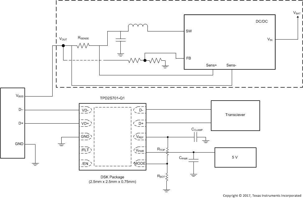
The TPD2S701-Q1 also has the ability to vary the OVP threshold based on the configuration of the Mode pin and the voltage present on the VREF pin (0.6 V-4.5 V). This functionality is discussed in greater depth in the OVP Threshold section. Once the VREF threshold is crossed, a fault is detectable to the user through the FLT pin, where 5 V on the pin indicates no fault is detected, and 0 V-0.4 V represents a fault condition. Figure 21 shows the TPD2S701-Q1 in a typical application, interfacing between the protected internal circuitry and the connector side, where ESD vulnerability is at its highest.
9.2 Typical Application
 Figure 21. USB 2.0 Port With Short-to-VBUS and IEC ESD Protection
9.2.1 Design Requirements
9.2.1.1 Device Operation
Table 1 gives the complete device functionality in response to the EN pin, to overvoltage conditions at the connector (VD± pins), to thermal shutdown, and to the conditions of the VPWR, VREF, and MODE pins.
Table 1. Device Operation Table
| Functional Mode | EN | MODE | VREF | VPWR | VD± | TJ | FLT | Comments |
|---|---|---|---|---|---|---|---|---|
| NORMAL OPERATION | ||||||||
| Mode 0 unpowered 1 | X | Rbot ≤ 2.6 kΩ | X | X | X | X | H | Device unpowered, data switches open |
| Mode 0 unpowered 2 | X | Rbot ≤ 2.6 kΩ | X | X | X | X | H | Device unpowered, data switches open |
| Mode 1 unpowered | X | Rtop | | Rbot > 14 kΩ | X | X | X | X | H | Device unpowered, data switches open |
| Mode 0 disabled | H | Rbot ≤ 2.6 kΩ | >UVLO | >UVLO | X | <TSD | H | Device disabled, data switches open |
| Mode 1 disabled | H | Rtop | | Rbot > 14 kΩ | Set by Rtop and Rbot | >UVLO | X | <TSD | H | Device disabled, data switches open, VREF is disabled |
| Mode 0 enabled | L | Rbot ≤ 2.6 kΩ | >UVLO | >UVLO | <OVP | <TSD | H | Device enabled, data switches closed, VREF is the value set by the power supply on VREF |
| Mode 1 enabled | L | Rtop | | Rbot > 14 kΩ | Set by Rtop and Rbot | >UVLO | <OVP | <TSD | H | Device enabled, data switches closed, VREF is the value set by the Rtop and Rbot resistor divider |
| FAULT CONDITIONS | ||||||||
| Mode 0 thermal shutdown | X | Rbot ≤ 2.6 kΩ | X | >UVLO | X | >TSD | L | Thermal shutdown, data switches opened, FLT pin asserted |
| Mode 1 thermal shutdown | X | Rtop | | Rbot > 14 kΩ | Set by Rtop and Rbot | >UVLO | X | >TSD | L | Thermal shutdown, data switches opened, VREF is disabled, FLT pin asserted |
| Mode 0 OVP fault | L | Rbot ≤ 2.6 kΩ | >UVLO | >UVLO | >OVP | <TSD | L | Data line overvoltage protection mode. OVP is set relative to the voltage on VREF. Data switches opened, FLT pin asserted |
| Mode 1 OVP fault | L | Rtop | | Rbot > 14 kΩ | Set by Rtop and Rbot | >UVLO | >OVP | <TSD | L | Data line overvoltage protection mode. OVP is set relative to the voltage on VREF. Data switches opened, fault pin asserted |
9.2.2 Detailed Design Procedure
9.2.2.1 VREF Operation
The TPD2S701-Q1 has two modes of operation which vary the way the VREF pin functions. In Mode 0, the VREF pin is connected to an external regulator which sets the voltage on the VREF pin. In Mode 1, the TPD2S701-Q1 uses an adjustable internal regulator to set the VREF voltage. Mode 1 enables the system designer to operate the TPD2S701-Q1 with a single power supply, and have the flexibility to easily set the VREF voltage to any voltage between 0.6 V and 3.8 V with two external resistors.
9.2.2.1.1 Mode 0
To set the device into Mode 0, ensure that Rbot, resistance between the MODE pin and ground, is less than 2.6 kΩ. The easiest way to implement Mode 0 is to directly connect the mode pin to GND on your PCB. With this resistance condition met, connect VREF to an external regulator to set the VREF voltage.
9.2.2.1.2 Mode 1
To operate in Mode 1, ensure that Rtop || Rbot, resistance between the MODE pin and ground, is greater than 14 kΩ. This is accomplished by insuring Rtop || Rbot > 14 kΩ because when the device is initially powered up, VREF is at ground until the internal circuitry recognizes if the device is in Mode 1 or Mode 2.
In Mode 1, VREF is set by using an internal regulator to set the voltage. Using a resistor divider off of a feedback comparator is how to set VREF, similar to a standard LDO or DC/DC. VREF is set in Mode 1 according to Equation 5.

Equation 5 yields the typical value for VREF. When using ±1% resistors RTOP and RBOT, VREF accuracy is going to be ±5%. Therefore, the minimum and maximum values for VREF can be calculated off of the typical VREF. The parametric tables above give example RTOP and RBOT resistors to use for standard output VREF voltages for Mode 1.
9.2.2.2 Mode 1 Enable Timing
In Mode 1, when the TPD2S701-Q1 is disabled, the output regulator is disabled, leading VREF to discharge to 0 V through RTOP and RBOT. It is desired for VREF to be at 0 V when the device is disabled to minimize the clamping voltage during a power disabled ESD event. If VREF is at 0 V, this holds D± near ground during these fault events.
When enabling the TPD2S701-Q1, VREF is quickly charged up to insure a quick turnon time of the Data FETs. Data FET turnon is gated by VREF reaching 80% of its final voltage plus 150 µs to insure a proper OVP threshold is set before passing data. This prevents false OVPs due to normal operation. Because Data FET turnon is gated by charging the VREF clamping capacitor, the size of the capacitor influences the turnon time of the Data switches. The TPD2S701-Q1’s internal regulator uses a constant current source to quickly charge the VREF clamping capacitor, so the charging time of CVREF can easily be calculated with Equation 6.

Where CVREF is the clamping capacitance on VREF, VREFFINAL is the final value VREF is set to, and ICHG_VREF = 22 mA (typical). If VREF = 1 V, 0.8 is used in the above equation because 80% of VREF is the amount of time that gates the turnon of the Data FETs. Once tCHG_CVREF is calculated, the typical turnon time of the Data FETs can be calculated from Equation 7.

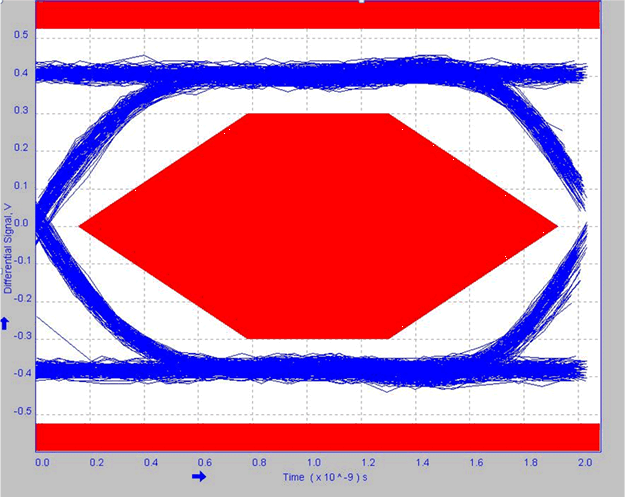
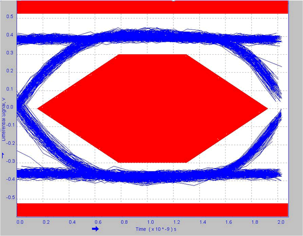
9.2.3 Application Curves

