JAJSDL7D January 2016 – May 2021 TPS61194
PRODUCTION DATA
- 1 特長
- 2 アプリケーション
- 3 概要
- 4 Revision History
- 5 Pin Configuration and Functions
-
6 Specifications
- 6.1 Absolute Maximum Ratings
- 6.2 ESD Ratings
- 6.3 Recommended Operating Conditions
- 6.4 Thermal Information
- 6.5 Electrical Characteristics (1) (1)
- 6.6 Internal LDO Electrical Characteristics
- 6.7 Protection Electrical Characteristics
- 6.8 Current Sinks Electrical Characteristics
- 6.9 PWM Brightness Control Electrical Characteristics
- 6.10 Boost and SEPIC Converter Characteristics
- 6.11 Logic Interface Characteristics
- 6.12 Typical Characteristics
- 7 Detailed Description
- 8 Application and Implementation
- 9 Power Supply Recommendations
- 10Layout
- 11Device and Documentation Support
- 12Mechanical, Packaging, and Orderable Information
7.3.4.2 Overview of the Fault/Protection Schemes
A summary of the TPS61194fault detection behavior is shown in Table 7-3. Detected faults (excluding LED open or short) cause device to enter FAULT_RECOVERY state. In FAULT_RECOVERY the DC-DC and LED current sinks of the device are disabled, and the FAULT pin is pulled low. The device recovers automatically and enters normal operating mode (ACTIVE) after a recovery time of 100 ms if the fault condition has disappeared. When recovery is succesful, FAULT pin is released.
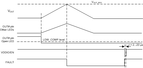
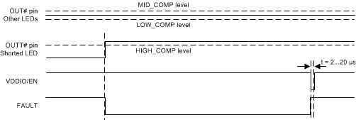
If a LED fault is detected, the device continues normal operation and only the faulty string is disabled. The fault is indicated via the FAULT pin which can be released by toggling VDDIO/EN pin low for a short period of 2 µs to 20 µs. LEDs are turned off for this period but the device stays in ACTIVE mode. If VDDIO/EN is low longer, the device goes to STANDBY and restarts when EN goes high again.
| FAULT/ PROTECTION | FAULT NAME | THRESHOLD | FAULT PIN | FAULT_ RECOVERY STATE | ACTION |
|---|---|---|---|---|---|
| VIN overvoltage protection | VIN_OVP | 1. VIN > 42 V 2. VOUT > VSET_DCDC + 6..10 V. VSET_DCDC is voltage value defined by logic during adaptation | Yes | Yes | 1. Overvoltage is monitored from the beginning of soft start. Fault
is detected if the duration of overvoltage condition is 100 µs
minimum. 2. Overvoltage is monitored from the beginning of normal operation (ACTIVE mode). Fault is detected if over-voltage condition duration is 560 ms minimum (tfilter). After the first fault, detection filter time is reduced to 50 ms for following recovery cycles. When the device recovers and has been in ACTIVE mode for 160 ms, filter time is increased back to 560 ms. |
| VIN undervoltage lockout | VIN_UVLO | Falling 3.9 V Rising 4 V | Yes | Yes | Detects undervoltage condition at VIN pin. Sensed in all operating modes. Fault is detected if undervoltage condition duration is 100 µs minimum. |
| Open LED fault | OPEN_LED | LOW_COMP threshold | Yes | No | Detected if the voltage of one or more current sinks is below threshold level, and DC-DC adaptive control has reached maximum voltage. Open string is removed from the DC-DC voltage control loop and current sink is disabled. Fault pin is released by toggling VDDIO/EN pin. If VDDIO/EN is low for a period of 2 µs to 20 µs, LEDs are turned off for this period but device stays ACTIVE. If VDDIO/EN is low longer, device goes to STANDBY and restarts when EN goes high again. |
| Shorted LED fault | SHORT_LED | Shorted string detection level 6 V | Yes | No | Detected if the voltage of one or more current sinks is above
shorted string detection level and at least one OUTx voltage is
within headroom window. Shorted string is removed from the DC-DC
voltage control loop and current sink is disabled. Fault pin is released by toggling VDDIO/EN pin. If VDDIO/EN is low for a period of 2…20 µs, LEDs are turned off for this period but device stays ACTIVE. If VDDIO/EN is low longer, device goes to STANDBY and restarts when EN goes high again. |
| Thermal protection | TSD | 165°C Thermal shutdown hysteresis 20°C | Yes | Yes | Thermal shutdown is monitored from the beginning of soft start. Die temperature must decrease by 20°C for device to recover. |
 Figure 7-5 VIN Overvoltage Protection (DC-DC OVP)
 Figure 7-6 VIN Overvoltage Protection (VIN OVP)
 Figure 7-7 VIN Undervoltage Lockout
 Figure 7-8 LED Open Fault
 Figure 7-9 LED Short Fault