JAJSDL7D January 2016 – May 2021 TPS61194
PRODUCTION DATA
- 1 特長
- 2 アプリケーション
- 3 概要
- 4 Revision History
- 5 Pin Configuration and Functions
-
6 Specifications
- 6.1 Absolute Maximum Ratings
- 6.2 ESD Ratings
- 6.3 Recommended Operating Conditions
- 6.4 Thermal Information
- 6.5 Electrical Characteristics (1) (1)
- 6.6 Internal LDO Electrical Characteristics
- 6.7 Protection Electrical Characteristics
- 6.8 Current Sinks Electrical Characteristics
- 6.9 PWM Brightness Control Electrical Characteristics
- 6.10 Boost and SEPIC Converter Characteristics
- 6.11 Logic Interface Characteristics
- 6.12 Typical Characteristics
- 7 Detailed Description
- 8 Application and Implementation
- 9 Power Supply Recommendations
- 10Layout
- 11Device and Documentation Support
- 12Mechanical, Packaging, and Orderable Information
7.3.4.1 Adaptive DC-DC Voltage Control and Functionality of LED Fault Comparators
Adaptive voltage control function adjusts the DC-DC output voltage to the minimum sufficient voltage for proper LED current sink operation. The current sink with highest VF LED string is detected and DC-DC output voltage adjusted accordingly. DC-DC adaptive control voltage step size is defined by maximum voltage setting, VSTEP = (VOUT_MAX – VOUT_MIN) / 256. Periodic down pressure is applied to the target voltage to achieve better system efficiency.
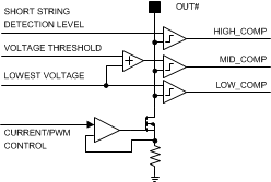
Every LED current sink has 3 comparators for the adaptive DC-DC control and LED fault detections. Comparator outputs are filtered, filtering time is 1 µs.
 Figure 7-3 Comparators for Adaptive Voltage Control and LED Fault Detection
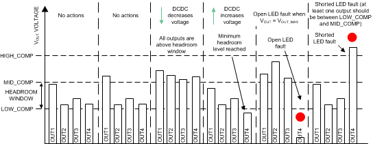
Figure 7-4 shows different cases which cause DC-DC voltage increase, decrease, or generate faults. In normal operation voltage at all the OUT# pins is between LOW_COMP and MID_COMP levels, and boost voltage stays constant. LOW_COMP level is the minimum for proper LED current sink operation, 1.1 × VSAT + 0.2 V (typical). MID_COMP level is 1.1 × VSAT + 1.2 V (typical) so typical headroom window is 1 V.
When voltage at all the OUT# pins increases above MID_COMP level, DC-DC voltage adapts downwards.
When voltage at any of the OUT# pins falls below LOW_COMP threshold, DC-DC voltage adapts upwards. In the condition where DC-DC voltage reaches the maximum and there are one or more outputs still below LOW_COMP level, an open LED fault is detected.
HIGH_COMP level, 6 V typical, is the threshold for shorted LED detection. When the voltage of one or more of the OUT# pins increases above HIGH_COMP level and at least one of the other outputs is within the normal headroom window, shorted LED fault is detected.
 Figure 7-4 Protection and DC-DC Voltage Adaptation Algorithms