JAJSDM6B July   2017  – August 2024 ESD401

PRODUCTION DATA  

  1.   1
  2. 特長
  3. アプリケーション
  4. 概要
  5. Pin Configuration and Functions
  6. Specifications
    1. 5.1 Absolute Maximum Ratings
    2. 5.2 ESD Ratings — JEDEC Specification 
    3. 5.3 ESD Ratings—IEC Specification
    4. 5.4 Recommended Operating Conditions
    5. 5.5 Thermal Information
    6. 5.6 Electrical Characteristics
    7. 5.7 Typical Characteristics
  7. Detailed Description
    1. 6.1 Overview
    2. 6.2 Functional Block Diagram
    3. 6.3 Feature Description
      1. 6.3.1 IEC 61000-4-2 ESD Protection
      2. 6.3.2 IEC 61000-4-4 EFT Protection
      3. 6.3.3 IEC 61000-4-5 Surge Protection
      4. 6.3.4 IO Capacitance
      5. 6.3.5 DC Breakdown Voltage
      6. 6.3.6 Low Leakage Current
      7. 6.3.7 Low ESD Clamping Voltage
      8. 6.3.8 Industrial Temperature Range
      9. 6.3.9 Industry Standard Footprint
    4. 6.4 Device Functional Modes
  8. Application and Implementation
    1. 7.1 Application Information
    2. 7.2 Typical Application
      1. 7.2.1 Design Requirements
      2. 7.2.2 Detailed Design Procedure
        1. 7.2.2.1 Signal Range
        2. 7.2.2.2 Operating Frequency
      3. 7.2.3 Application Curves
    3. 7.3 Power Supply Recommendations
    4. 7.4 Layout
      1. 7.4.1 Layout Guidelines
      2. 7.4.2 Layout Example
  9. Device and Documentation Support
    1. 8.1 ドキュメントの更新通知を受け取る方法
    2. 8.2 サポート・リソース
    3. 8.3 Trademarks
    4. 8.4 静電気放電に関する注意事項
    5. 8.5 用語集
  10. Revision History
  11. 10Mechanical, Packaging, and Orderable Information
    1. 10.1 Tape and Reel Information
  12. 11Mechanical Data

Pin Configuration and Functions

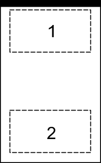
ESD401 DPY
                        Package,2-Pin X1SON(Top View)Figure 4-1 DPY Package,2-Pin X1SON(Top View)
Table 4-1 Pin Functions
PIN TYPE(1) DESCRIPTION
NAME NO.
IO 1 I/O ESD Protected Channel. If used as ESD IO, connect pin 2 to ground
IO 2 I/O ESD Protected Channel. If used as ESD IO, connect pin 1 to ground
I = input, O = output