JAJSDP5D February   2016  – March 2018 LM36273

PRODUCTION DATA.  

  1. 特長
  2. アプリケーション
    1.     概略回路図
  3. 概要
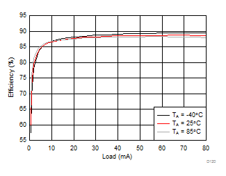
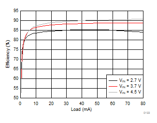
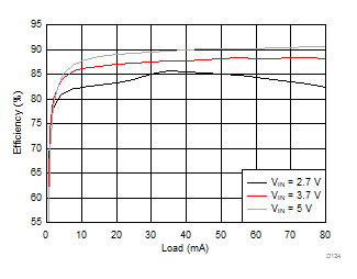
    1.     バックライト効率、3P7S
  4. 改訂履歴
  5. Pin Configuration and Functions
    1.     Pin Functions
  6. Specifications
    1. 6.1 Absolute Maximum Ratings
    2. 6.2 ESD Ratings
    3. 6.3 Recommended Operating Conditions
    4. 6.4 Thermal Information
    5. 6.5 Electrical Characteristics
    6. 6.6 I2C Timing Requirements (Fast Mode)
    7. 6.7 Typical Characteristics
  7. Detailed Description
    1. 7.1 Overview
    2. 7.2 Functional Block Diagram
    3. 7.3 Features Description
      1. 7.3.1 Enabling the LM36273
      2. 7.3.2 Backlight
        1. 7.3.2.1 Current Sink Enable
        2. 7.3.2.2 Brightness Mapping
          1. 7.3.2.2.1 Linear Mapping
          2. 7.3.2.2.2 Exponential Mapping
        3. 7.3.2.3 Backlight Brightness Control Modes
          1. 7.3.2.3.1 I2C Brightness Control (PWM Pin Disabled)
          2. 7.3.2.3.2 I2C × PWM Brightness Control (PWM Pin Enabled)
            1. 7.3.2.3.2.1 PWM Ramper
        4. 7.3.2.4 Boost Switching Frequency
          1. 7.3.2.4.1 Minimum Inductor Select
        5. 7.3.2.5 Boost Feedback Gain Select
        6. 7.3.2.6 Auto Switching Frequency
        7. 7.3.2.7 PWM Input
          1. 7.3.2.7.1 PWM Sample Frequency
            1. 7.3.2.7.1.1 PWM Resolution and Input Frequency Range
            2. 7.3.2.7.1.2 PWM Sample Rate and Efficiency
              1. 7.3.2.7.1.2.1 PWM Sample Rate Example
          2. 7.3.2.7.2 PWM Hysteresis
          3. 7.3.2.7.3 PWM Step Response
          4. 7.3.2.7.4 PWM Timeout
          5. 7.3.2.7.5 PWM-to-Digital Code Readback
        8. 7.3.2.8 Regulated Headroom Voltage
        9. 7.3.2.9 Backlight Fault Protection and Faults
          1. 7.3.2.9.1 Backlight Overvoltage Protection (OVP)
          2. 7.3.2.9.2 Backlight Overcurrent Protection (OCP)
      3. 7.3.3 LCM Bias
        1. 7.3.3.1 Display Bias Boost Converter (VVPOS, VVNEG)
        2. 7.3.3.2 Auto Sequence Mode
        3. 7.3.3.3 Wake-up Mode
          1. 7.3.3.3.1 Wake1 Mode
          2. 7.3.3.3.2 Wake2 Mode
        4. 7.3.3.4 Active Discharge
        5. 7.3.3.5 LCM Bias Protection and Faults
          1. 7.3.3.5.1 LCM Overvoltage (OVP) Protection
          2. 7.3.3.5.2 VPOS Short-Circuit Protection
          3. 7.3.3.5.3 VNEG Short-Circuit Protection
      4. 7.3.4 Software Reset
      5. 7.3.5 HWEN Input
      6. 7.3.6 Thermal Shutdown (TSD)
    4. 7.4 Device Functional Modes
      1. 7.4.1 Modes of Operation
    5. 7.5 Programming
      1. 7.5.1 I2C-Compatible Serial Bus Interface
        1. 7.5.1.1 Interface Bus Overview
        2. 7.5.1.2 Data Transactions
        3. 7.5.1.3 Acknowledge Cycle
        4. 7.5.1.4 Acknowledge After Every Byte Rule
        5. 7.5.1.5 Addressing Transfer Formats
        6. 7.5.1.6 Register Programming
    6. 7.6 Register Maps
      1. 7.6.1  Revision Register (Address = 0x01)[Reset = 0x01]
        1. Table 11. Revision Register Field Descriptions
      2. 7.6.2  Backlight Configuration1 Register (Address = 0x02)[Reset = 0x28]
        1. Table 12. Backlight Configuration 1 Register Field Descriptions
      3. 7.6.3  Backlight Configuration 2 Register (Address = 0x03)[Reset = 0x8D]
        1. Table 13. Backlight Configuration 2 Register Field Descriptions
      4. 7.6.4  Backlight Brightness LSB Register (Address = 0x04)[Reset = 0x07]
        1. Table 14. Backlight Brightness LSB Register Field Descriptions
      5. 7.6.5  Backlight Brightness MSB Register (Address = 0x05)[Reset = 0xFF]
        1. Table 15. Backlight Brightness MSB Register Field Descriptions
      6. 7.6.6  Backlight Auto-Frequency Low Threshold Register (Address = 0x06)[Reset = 0x00]
        1. Table 16. Backlight Auto-Frequency Low Threshold Field Descriptions
      7. 7.6.7  Backlight Auto-Frequency High Threshold Register (Address = 0x07)[Reset = 0x00]
        1. Table 17. Backlight Auto-Frequency High Threshold Field Descriptions
      8. 7.6.8  Backlight Enable Register (Address = 0x08)[Reset = 0x00]
        1. Table 18. Backlight Enable Register Field Descriptions
      9. 7.6.9  Bias Configuration 1 Register (Address = 0x09)[Reset = 0x18]
        1. Table 19. Bias Configuration 1 Register Field Descriptions
      10. 7.6.10 Bias Configuration 2 register (Address = 0x0A)[Reset = 0x11]
        1. Table 20. Bias Configuration 2 Register Field Descriptions
      11. 7.6.11 Bias Configuration 3 Register (Address = 0x0B)[Reset = 0x00]
        1. Table 21. Bias Configuration 3 Register Field Descriptions
      12. 7.6.12 LCM Boost Bias Register (Address = 0x0C)[Reset = 0x28]
        1. Table 22. LCM Boost Bias Register Field Descriptions
      13. 7.6.13 VPOS Bias Register (Address = 0x0D)[Reset = 0x1E]
        1. Table 23. VPOS Bias Register Field Descriptions
      14. 7.6.14 VNEG Bias Register (Address = 0x0E)[Reset = 0x1C]
        1. Table 24. VNEG Bias Register Field Descriptions
      15. 7.6.15 Flags Register (Address = 0x0F)[Reset = 0x00]
        1. Table 25. Flags Register Field Descriptions
      16. 7.6.16 Option 1 Register (Address = 0x10)[Reset = 0x06]
        1. Table 26. Option 1 Register Field Descriptions
      17. 7.6.17 Option 2 Register (Address = 0x11)[Reset = 0x35]
        1. Table 27. Option 2 Register Field Descriptions
      18. 7.6.18 PWM-to-Digital Code Readback LSB Register (Address = 0x12)[Reset = 0x00]
        1. Table 28. PWM-to-Digital Code Readback LSB Register Field Descriptions
      19. 7.6.19 PWM-to-Digital Code Readback MSB Register (Address = 0x13)[Reset = 0x00]
        1. Table 29. PWM-to-Digital Code Readback MSB Register Field Descriptions
  8. Application and Implementation
    1. 8.1 Application Information
    2. 8.2 Typical Application
      1. 8.2.1 Design Requirements
      2. 8.2.2 Detailed Design Procedure
        1. 8.2.2.1 Component Selection
          1. 8.2.2.1.1 Inductor Selection
          2. 8.2.2.1.2 Boost Output Capacitor Selection
          3. 8.2.2.1.3 Input Capacitor Selection
      3. 8.2.3 Application Curves
        1. 8.2.3.1 Backlight Curves
          1. 8.2.3.1.1 Two LED Strings
          2. 8.2.3.1.2 Three LED Strings
        2. 8.2.3.2 LCM Bias Curves
  9. Power Supply Recommendations
  10. 10Layout
    1. 10.1 Layout Guidelines
    2. 10.2 Layout Example
  11. 11デバイスおよびドキュメントのサポート
    1. 11.1 デバイス・サポート
      1. 11.1.1 デベロッパー・ネットワークの製品に関する免責事項
      2. 11.1.2 開発サポート
    2. 11.2 ドキュメントのサポート
      1. 11.2.1 関連資料
    3. 11.3 ドキュメントの更新通知を受け取る方法
    4. 11.4 コミュニティ・リソース
    5. 11.5 商標
    6. 11.6 静電気放電に関する注意事項
    7. 11.7 Glossary
  12. 12メカニカル、パッケージ、および注文情報

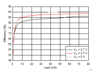
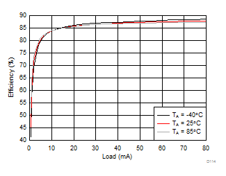
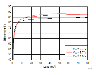
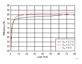
LCM Bias Curves

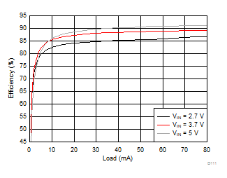
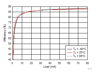
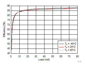
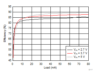
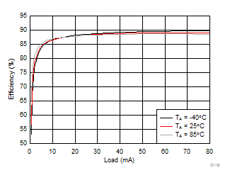
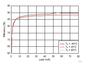
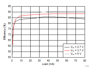
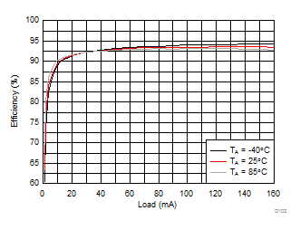
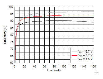
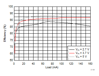
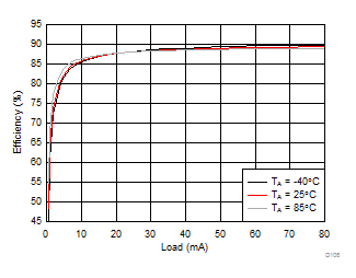
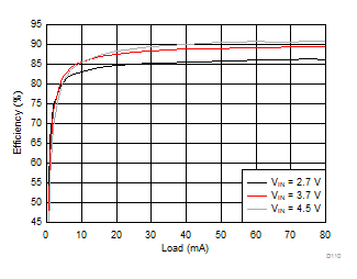
Ambient temperature is 25°C and VIN is 3.7 V unless otherwise noted. VPOS, VNEG and VPOS/VNEG efficiency is defined as POUT / PIN, where POUT is actual power consumed in VPOS, VNEG and (VPOS + VNEG) outputs, respectively. External components are from Table 30.
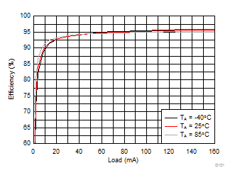
LM36273 D101_SNVSAC0.gif
VLCM_OUT = 4.3 V
Figure 151. LCM Boost Efficiency
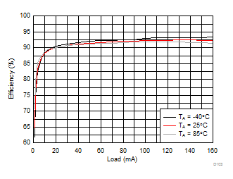
LM36273 D103_SNVSAC0.gif
VLCM_OUT = 6.3 V
Figure 153. LCM Boost Efficiency
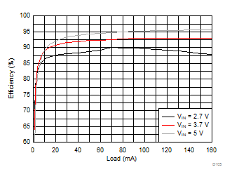
LM36273 D105_SNVSAC0.gif
VLCM_OUT = 5.8 V
Figure 155. LCM Boost Efficiency
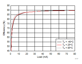
LM36273 D107_SNVSAC0.gif
VVPOS = 4 V VLCM_OUT = 4.3 V
Figure 157. VPOS Efficiency
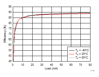
LM36273 D109_SNVSAC0.gif
VVPOS = 6 V VLCM_OUT = 6.3 V
Figure 159. VPOS Efficiency
LM36273 D111_SNVSAC0.gif
VVPOS = 6 V VLCM_OUT = 6.3 V
Figure 161. VPOS Efficiency
LM36273 D113_SNVSAC0.gif
VVNEG = -4 V VLCM_OUT = 4.3 V
Figure 163. VNEG Efficiency
LM36273 D115_SNVSAC0.gif
VVNEG = -6 V VLCM_OUT = 6.3 V
Figure 165. VNEG Efficiency
LM36273 D117_SNVSAC0.gif
VVNEG = –5.5 V VLCM_OUT = 5.8 V
Figure 167. VNEG Efficiency
LM36273 D119_SNVSAC0.gif
VVPOS = 4 V VVNEG = –4 V VLCM_OUT = 4.3 V
Figure 169. VPOS/VNEG Efficiency
LM36273 D121_SNVSAC0.gif
VVPOS = 6 V VVNEG = –6 V VLCM_OUT = 6.3 V
Figure 171. VPOS/VNEG Efficiency
LM36273 D123_SNVSAC0.gif
VVPOS = 5.5 V VVNEG = –5.5 V VLCM_OUT = 5.8 V
Figure 173. VPOS/VNEG Efficiency
LM36273 D102_SNVSAC0.gif
VLCM_OUT = 5.3 V
Figure 152. LCM Boost Efficiency
LM36273 D104_SNVSAC0.gif
VLCM_OUT = 4.8 V
Figure 154. LCM Boost Efficiency
LM36273 D106_SNVSAC0.gif
VLCM_OUT = 6.8 V
Figure 156. LCM Boost Efficiency
LM36273 D108_SNVSAC0.gif
VVPOS = 5 V VLCM_OUT = 5.3 V
Figure 158. VPOS Efficiency
LM36273 D110_SNVSAC0.gif
Figure 160. VPOS Efficiency
LM36273 D112_SNVSAC0.gif
VVPOS = 6.5 V VLCM_OUT = 6.8 V
Figure 162. VPOS Efficiency
LM36273 D114_SNVSAC0.gif
VVNEG = -5 V VLCM_OUT = 5.3 V
Figure 164. VNEG Efficiency
LM36273 D116_SNVSAC0.gif
VVNEG = –4.5 V VLCM_OUT = 4.8 V
Figure 166. VNEG Efficiency
LM36273 D118_SNVSAC0.gif
VVNEG = –6.5 V VLCM_OUT = 6.8 V
Figure 168. VNEG Efficiency
LM36273 D120_SNVSAC0.gif
VVPOS = 5 V VVNEG = –5 V VLCM_OUT = 5.3 V
Figure 170. VPOS/VNEG Efficiency
LM36273 D122_SNVSAC0.gif
VVPOS = 4.5 V VVNEG = –4.5 V VLCM_OUT = 4.8 V
Figure 172. VPOS/VNEG Efficiency
LM36273 D124_SNVSAC0.gif
VVPOS = 6.5 V VVNEG = –6.5 V VLCM_OUT = 6.8 V
Figure 174. VPOS/VNEG Efficiency