JAJSDP5D February 2016 – March 2018 LM36273
PRODUCTION DATA.
- 1 特長
- 2 アプリケーション
- 3 概要
- 4 改訂履歴
- 5 Pin Configuration and Functions
- 6 Specifications
-
7 Detailed Description
- 7.1 Overview
- 7.2 Functional Block Diagram
- 7.3
Features Description
- 7.3.1 Enabling the LM36273
- 7.3.2 Backlight
- 7.3.3 LCM Bias
- 7.3.4 Software Reset
- 7.3.5 HWEN Input
- 7.3.6 Thermal Shutdown (TSD)
- 7.4 Device Functional Modes
- 7.5 Programming
- 7.6
Register Maps
- 7.6.1 Revision Register (Address = 0x01)[Reset = 0x01]
- 7.6.2 Backlight Configuration1 Register (Address = 0x02)[Reset = 0x28]
- 7.6.3 Backlight Configuration 2 Register (Address = 0x03)[Reset = 0x8D]
- 7.6.4 Backlight Brightness LSB Register (Address = 0x04)[Reset = 0x07]
- 7.6.5 Backlight Brightness MSB Register (Address = 0x05)[Reset = 0xFF]
- 7.6.6 Backlight Auto-Frequency Low Threshold Register (Address = 0x06)[Reset = 0x00]
- 7.6.7 Backlight Auto-Frequency High Threshold Register (Address = 0x07)[Reset = 0x00]
- 7.6.8 Backlight Enable Register (Address = 0x08)[Reset = 0x00]
- 7.6.9 Bias Configuration 1 Register (Address = 0x09)[Reset = 0x18]
- 7.6.10 Bias Configuration 2 register (Address = 0x0A)[Reset = 0x11]
- 7.6.11 Bias Configuration 3 Register (Address = 0x0B)[Reset = 0x00]
- 7.6.12 LCM Boost Bias Register (Address = 0x0C)[Reset = 0x28]
- 7.6.13 VPOS Bias Register (Address = 0x0D)[Reset = 0x1E]
- 7.6.14 VNEG Bias Register (Address = 0x0E)[Reset = 0x1C]
- 7.6.15 Flags Register (Address = 0x0F)[Reset = 0x00]
- 7.6.16 Option 1 Register (Address = 0x10)[Reset = 0x06]
- 7.6.17 Option 2 Register (Address = 0x11)[Reset = 0x35]
- 7.6.18 PWM-to-Digital Code Readback LSB Register (Address = 0x12)[Reset = 0x00]
- 7.6.19 PWM-to-Digital Code Readback MSB Register (Address = 0x13)[Reset = 0x00]
- 8 Application and Implementation
- 9 Power Supply Recommendations
- 10Layout
- 11デバイスおよびドキュメントのサポート
- 12メカニカル、パッケージ、および注文情報
7.3.2.1 Current Sink Enable
Each current sink in the device has a separate enable input. This allows for a one-string, two-string or three-string application. Once the correct LED string configuration is programmed and a non-zero code is written to the brightness registers, the device can be enabled by writing the backlight enable bit high (register 0x08 bit[4]).
The default settings for the device are backlight enable bit set to 0, all backlight strings disabled, PWM input disabled, linear mapped mode, and the brightness level set to 30 mA per string.
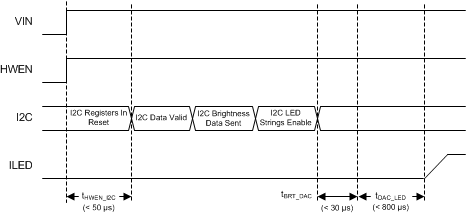
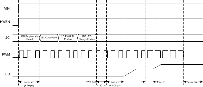
When PWM is enabled, the LM36273 actively monitors the PWM input. After a non-zero PWM duty cycle is detected, the LM36273 multiplies the duty cycle with the programmed I2C brightness code to give an 11-bit brightness value between 60 µA and 30 mA. Figure 31 and Figure 32 describe the start-up timing for operation with I2C controlled current and with PWM controlled current.
 Figure 31. Enabling the LM36273 via I2C
 Figure 32. Enabling the LM36273 via PWM
The LM36273 backlight can be enabled or disabled in various ways. When disabled, the device is considered shut down, and the quiescent current drops to ISHDN. When the device is in standby, it returns to the ISTANDBY current level retaining all programmed register values. Table 1 describes the different backlight operating states for the LM36273.
Table 1. Backlight Operating Modes
| HWEN | BL_EN
0x08[4] |
PWM INPUT | I2C BRIGHTNESS
0x05[7:0] 0x04[2:0] |
CURRENT SINK ENABLES
0x08[2:0] |
PWM EN
0x02[0] |
PWM RAMP
0x02[1] |
FEEDBACK DISABLES
0x10[5:3] |
MAPPING MODE
0x02[3] |
ACTION |
|---|---|---|---|---|---|---|---|---|---|
| 0 | X | X | X | X | X | X | X | X | Shutdown |
| 1 | 0 | X | X | X | X | X | X | X | Standby(1) |
| 1 | 1 | X | 0x000 | 000 | X | X | X | X | Standby(1) |
| 1 | 1 | X | ≥0x001 | ≥001 | 0 | X | <111 | 0 = Exponential Mode
1 = Linear Mode |
-Backlight boost enabled
-Selected current sink(s) enabled -I2C control only |
| 1 | 1 | Duty cycle = 0 | X | ≥001 | 1 | X | <111 | X | Standby(1) |
| 1 | 1 | Duty cycle > 0 | ≥0x001 | ≥001 | 1 | 0 | <111 | 0 = Exponential Mode
1 = Linear Mode |
-Backlight boost enabled
-Selected current sink(s) enabled -I2C × PWM (after ramper) -No ramp between PWM duty-cycle change |
| 1 | 1 | Duty cycle > 0 | ≥0x001 | ≥001 | 1 | 1 | <111 | 0 = Exponential Mode
1 = Linear Mode |
-Backlight boost enabled
-Selected current sink(s) enabled -I2C × PWM (before ramper) |
| 1 | 1 | Duty cycle > 0 | ≥0x001 | ≥001 | 1 | 0 | 111 | 0 = Exponential Mode
1 = Linear Mode |
-Backlight boost disabled
-Selected current sink(s) enabled -I2C × PWM (after ramper) |
| 1 | 1 | Duty cycle > 0 | ≥0x001 | ≥001 | 1 | 1 | 111 | 0 = Exponential Mode
1 = Linear Mode |
-Backlight boost disabled
-Selected current sink(s) enabled -I2C × PWM (before ramper) |