JAJSDS8C September   2017  – May 2019 TDP142

PRODUCTION DATA.  

  1. 特長
  2. アプリケーション
  3. 概要
    1.     Device Images
      1.      概略回路図
      2.      ディスプレイ
  4. 改訂履歴
  5. Pin Configuration and Functions
    1.     Pin Functions
  6. Specifications
    1. 6.1  Absolute Maximum Ratings
    2. 6.2  ESD Ratings
    3. 6.3  Recommended Operating Conditions
    4. 6.4  Thermal Information
    5. 6.5  Power Supply Characteristics
    6. 6.6  DC Electrical Characteristics
    7. 6.7  AC Electrical Characteristics
    8. 6.8  Timing Requirements
    9. 6.9  Switching Characteristics
    10. 6.10 Typical Characteristics
  7. Parameter Measurement Information
  8. Detailed Description
    1. 8.1 Overview
    2. 8.2 Functional Block Diagram
    3. 8.3 Feature Description
      1. 8.3.1 DisplayPort
      2. 8.3.2 4-level Inputs
      3. 8.3.3 Receiver Linear Equalization
    4. 8.4 Device Functional Modes
      1. 8.4.1 Device Configuration in GPIO Mode
      2. 8.4.2 Device Configuration In I2C Mode
      3. 8.4.3 Linear EQ Configuration
      4. 8.4.4 Operation Timing – Power Up
    5. 8.5 Programming
    6. 8.6 Register Maps
      1. 8.6.1 General Register (address = 0x0A) [reset = 00000001]
        1. Table 6. General Registers
      2. 8.6.2 DisplayPort Control/Status Registers (address = 0x10) [reset = 00000000]
        1. Table 7. DisplayPort Control/Status Registers (0x10)
      3. 8.6.3 DisplayPort Control/Status Registers (address = 0x11) [reset = 00000000]
        1. Table 8. DisplayPort Control/Status Registers (0x11)
      4. 8.6.4 DisplayPort Control/Status Registers (address = 0x12) [reset = 00000000]
        1. Table 9. DisplayPort Control/Status Registers (0x12)
      5. 8.6.5 DisplayPort Control/Status Registers (address = 0x13) [reset = 00000000]
        1. Table 10. DisplayPort Control/Status Registers (0x13)
  9. Application and Implementation
    1. 9.1 Application Information
    2. 9.2 Typical Application
      1. 9.2.1 Source Application Implementation
        1. 9.2.1.1 Design Requirement
        2. 9.2.1.2 Detail Design Procedure
      2. 9.2.2 Sink Application Implementation
        1. 9.2.2.1 Design Requirements
        2. 9.2.2.2 Detailed Design Procedure
      3. 9.2.3 Application Curve
  10. 10Power Supply Recommendations
  11. 11Layout
    1. 11.1 Layout Guidelines
    2. 11.2 Layout Example
  12. 12デバイスおよびドキュメントのサポート
    1. 12.1 関連リンク
    2. 12.2 ドキュメントの更新通知を受け取る方法
    3. 12.3 コミュニティ・リソース
    4. 12.4 商標
    5. 12.5 静電気放電に関する注意事項
    6. 12.6 Glossary
  13. 13メカニカル、パッケージ、および注文情報

Sink Application Implementation

Figure 19 is the schematic for the Sink application, and the left side of TDP142 is connected to DisplayPort receptacle and the right side of TDP142 is connected to Scaler or DisplayPort sink.
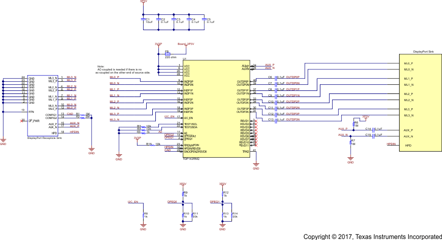
TDP142 sllsez1_app_sink.gifFigure 19. The Block diagram of DisplayPort Sink Application