JAJSE40A October 2017 – February 2018 UCC28780
PRODUCTION DATA.
- 1 特長
- 2 アプリケーション
- 3 概要
- 4 改訂履歴
- 5 Pin Configuration and Functions
- 6 Specifications
-
7 Detailed Description
- 7.1 Overview
- 7.2 Functional Block Diagram
- 7.3
Detailed Pin Description
- 7.3.1 BUR Pin (Programmable Burst Mode)
- 7.3.2 FB Pin (Feedback Pin)
- 7.3.3 VDD Pin (Device Bias Supply)
- 7.3.4 REF Pin (Internal 5-V Bias)
- 7.3.5 HVG and SWS Pins
- 7.3.6 RTZ Pin (Sets Delay for Transition Time to Zero)
- 7.3.7 RDM Pin (Sets Synthesized Demagnetization Time for ZVS Tuning)
- 7.3.8 RUN Pin (Driver Enable Pin)
- 7.3.9 SET Pin
- 7.4
Device Functional Modes
- 7.4.1 Adaptive ZVS Control with Auto-Tuning
- 7.4.2 Dead-Time Optimization
- 7.4.3 Control Law across Entire Load Range
- 7.4.4 Adaptive Amplitude Modulation (AAM)
- 7.4.5 Adaptive Burst Mode (ABM)
- 7.4.6 Low Power Mode (LPM)
- 7.4.7 Standby Power Mode (SBP)
- 7.4.8 Startup Sequence
- 7.4.9 Survival Mode of VDD
- 7.4.10 System Fault Protections
- 7.4.11 Pin Open/Short Protections
-
8 Application and Implementation
- 8.1 Application Information
- 8.2
Typical Application Circuit
- 8.2.1 Design Requirements
- 8.2.2 Detailed Design Procedure
- 8.2.3 Application Curves
- 9 Power Supply Recommendations
- 10Layout
- 11デバイスおよびドキュメントのサポート
- 12メカニカル、パッケージ、および注文情報
7.4.4 Adaptive Amplitude Modulation (AAM)
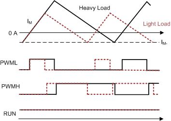
The switching pattern in AAM forces PWML and PWMH to alternate in a complementary fashion with dead-time in between, as shown in Figure 24. As the load current reduces, the negative magnetizing current (IM-) stays the same, while the positive magnetizing current (IM+) reduces by the internal peak current loop to regulate the output voltage. IM+ generates a current-feedback signal (VCS) on CS pin through a current-sense resistor (RCS) in series with QL, and a peak current threshold (VCST) in the current loop controls the peak current variation. Due to the nature of transition-mode (TM) operation, lowering the peak current with lighter load conditions results in higher switching frequency. When the load current increases to an over-power condition (IO(OPP)) where VCST correspondingly reaches an OPP threshold (VCST(OPP)) of the peak current loop, the OPP fault response will be triggered after a 160-ms timeout. The RUN signal stays high in AAM, so the half-bridge driver remains active.
 Figure 24. PWM Pattern in AAM