JAJSEC1C November   2019  – July 2020 ADS8686S

PRODUCTION DATA  

  1. 特長
  2. アプリケーション
  3. 概要
  4. Revision History
  5. Pin Configuration and Functions
  6. Specifications
    1. 6.1  Absolute Maximum Ratings
    2. 6.2  ESD Ratings
    3. 6.3  Recommended Operating Conditions
    4. 6.4  Thermal Information
    5. 6.5  Electrical Characteristics
    6. 6.6  Timing Requirements
    7. 6.7  Switching Characteristics
    8. 6.8  Timing Diagrams: Universal
    9. 6.9  Timing Diagrams: Parallel Data Read
    10. 6.10 Timing Diagrams: Serial Data Read
    11. 6.11 Typical Characteristics
  7. Detailed Description
    1. 7.1 Overview
    2. 7.2 Functional Block Diagram
    3. 7.3 Feature Description
      1. 7.3.1  Analog Inputs
      2. 7.3.2  Analog Input Impedance
      3. 7.3.3  Input Clamp Protection Circuit
      4. 7.3.4  Programmable Gain Amplifier (PGA)
      5. 7.3.5  Second-Order, Programmable, Low-Pass Filter (LPF)
      6. 7.3.6  ADC Driver
      7. 7.3.7  Multiplexer
      8. 7.3.8  Digital Filter and Noise
      9. 7.3.9  Reference
        1. 7.3.9.1 Internal Reference
        2. 7.3.9.2 External Reference
        3. 7.3.9.3 Supplying One VREF to Multiple Devices
      10. 7.3.10 ADC Transfer Function
    4. 7.4 Device Functional Modes
      1. 7.4.1 Device Interface: Pin Description
        1. 7.4.1.1  REFSEL (Input)
        2. 7.4.1.2  RESET (Input)
        3. 7.4.1.3  SEQEN (Input)
        4. 7.4.1.4  HW_RANGESEL[1:0] (Input)
        5. 7.4.1.5  SER/BYTE/PAR (Input)
        6. 7.4.1.6  DB[3:0] (Input/Output)
        7. 7.4.1.7  DB4/SER1W (Input/Output)
        8. 7.4.1.8  DB5/CRCEN (Input/Output)
        9. 7.4.1.9  DB[7:6] (Input/Output)
        10. 7.4.1.10 DB8 (Input/Output)
        11. 7.4.1.11 DB9/BYTESEL (Input/Output)
        12. 7.4.1.12 DB10/SDI (Input/Output)
        13. 7.4.1.13 DB11/SDOB (Input/Output)
        14. 7.4.1.14 DB12/SDOA (Input/Output)
        15. 7.4.1.15 DB13/OS0 (Input/Output)
        16. 7.4.1.16 DB14/OS1 (Input/Output)
        17. 7.4.1.17 DB15/OS2 (Input/Output)
        18. 7.4.1.18 WR/BURST (Input)
        19. 7.4.1.19 SCLK/RD (Input)
        20. 7.4.1.20 CS (Input)
        21. 7.4.1.21 CHSEL[2:0] (Input)
        22. 7.4.1.22 BUSY (Output)
        23. 7.4.1.23 CONVST (Input)
      2. 7.4.2 Device Modes of Operation
        1. 7.4.2.1 Shutdown Mode
        2. 7.4.2.2 Operation Mode
          1. 7.4.2.2.1 Hardware Mode
          2. 7.4.2.2.2 Software Mode
        3. 7.4.2.3 Reset Functionality
        4. 7.4.2.4 Channel Selection
          1. 7.4.2.4.1 Hardware Mode Channel Selection
          2. 7.4.2.4.2 Software Mode Channel Selection
        5. 7.4.2.5 Sequencer
          1. 7.4.2.5.1 Hardware Mode Sequencer
          2. 7.4.2.5.2 Software Mode Sequencer
        6. 7.4.2.6 Burst Sequencer
          1. 7.4.2.6.1 Hardware Mode Burst Sequencer
          2. 7.4.2.6.2 Software Mode Burst Sequencer
        7. 7.4.2.7 Diagnostics
          1. 7.4.2.7.1 Analog Diagnosis
          2. 7.4.2.7.2 Interface Diagnosis: SELF TEST and CRC
    5. 7.5 Programming
      1. 7.5.1 Parallel Interface
        1. 7.5.1.1 Reading Conversion Results
        2. 7.5.1.2 Writing Register Data
        3. 7.5.1.3 Reading Register Data
      2. 7.5.2 Parallel Byte Interface
        1. 7.5.2.1 Reading Conversion Results
        2. 7.5.2.2 Writing Register Data
        3. 7.5.2.3 Reading Register Data
      3. 7.5.3 Serial Interface
        1. 7.5.3.1 Reading Conversion Results
        2. 7.5.3.2 Writing Register Data
        3. 7.5.3.3 Reading Register Data
    6. 7.6 Register Maps
      1. 7.6.1 Page1 Registers
  8. Application and Implementation
    1. 8.1 Application Information
    2. 8.2 Typical Applications
      1. 8.2.1 8x2 Channel Data Acquisition System (DAQ) for Power Automation
        1. 8.2.1.1 Design Requirements
        2. 8.2.1.2 Detailed Design Procedure
        3. 8.2.1.3 Application Curve
      2. 8.2.2 Input Protection for Electrical Overstress
  9. Power Supply Recommendations
    1. 9.1 Power Supplies
  10. 10Layout
    1. 10.1 Layout Guidelines
    2. 10.2 Layout Examples
  11. 11Device and Documentation Support
    1. 11.1 Device Support
      1. 11.1.1 Development Support
    2. 11.2 Documentation Support
      1. 11.2.1 Related Documentation
    3. 11.3 Receiving Notification of Documentation Updates
    4. 11.4 サポート・リソース
    5. 11.5 Trademarks
    6. 11.6 Electrostatic Discharge Caution
    7. 11.7 Glossary

External Reference

For applications that require a reference voltage with a lower temperature drift or a common reference voltage for multiple devices, the ADS8686S offers a provision to use an external reference by using the internal buffer to drive the ADC reference. To select external reference mode, either tie the REFSEL pin low or connect this pin to DGND. In this mode, an external 2.5-V reference must be applied at REFIO (pin 33), which becomes a high-impedance input pin. Any low-drift, small-size external reference can be used in this mode because the internal buffer is optimally designed to handle the dynamic loading on the ADC reference input. The output of the external reference must be filtered to minimize the resulting effect of the reference noise on system performance. Figure 7-7 depicts a typical connection diagram for this mode.
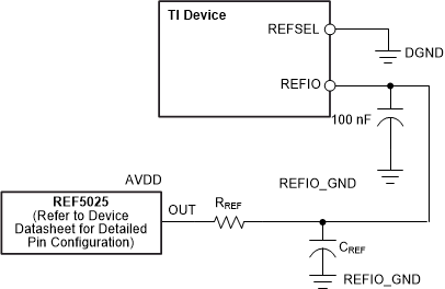
GUID-E8606CA2-985B-436E-A1F6-AB3DD6126E6A-low.gifFigure 7-7 Device Connections for Using an External 2.5-V Reference