JAJSEF5L July 2012 – May 2019 LP8556
PRODUCTION DATA.
- 1 特長
- 2 アプリケーション
- 3 概要
- 4 改訂履歴
- 5 Device Options
- 6 Pin Configuration and Functions
-
7 Specifications
- 7.1 Absolute Maximum Ratings
- 7.2 ESD Ratings
- 7.3 Recommended Operating Conditions
- 7.4 Thermal Information
- 7.5 Electrical Characteristics
- 7.6 Electrical Characteristics — Boost Converter
- 7.7 Electrical Characteristics — LED Driver
- 7.8 Electrical Characteristics — PWM Interface
- 7.9 Electrical Characteristics — Logic Interface
- 7.10 I2C Serial Bus Timing Parameters (SDA, SCL)
- 7.11 Typical Characteristics
-
8 Detailed Description
- 8.1 Overview
- 8.2 Functional Block Diagram
- 8.3
Feature Description
- 8.3.1 Boost Converter
- 8.3.2 Brightness Control
- 8.3.3 Fault Detection
- 8.4 Device Functional Modes
- 8.5 Programming
- 8.6
Register Maps
- 8.6.1 Register Bit Explanations
- 8.6.2
EPROM Bit Explanations
- 8.6.2.1 LP8556TM (DSBGA) Configurations and Pre-Configured EPROM Settings
- 8.6.2.2 LP8556TM (DSBGA) Configurations and Pre-configured EPROM Settings Continued
- 8.6.2.3 LP8556SQ (WQFN) Configurations and Pre-configured EPROM Settings
- 8.6.2.4 CFG98
- 8.6.2.5 CFG9E
- 8.6.2.6 CFG0
- 8.6.2.7 CFG1
- 8.6.2.8 CFG2
- 8.6.2.9 CFG3
- 8.6.2.10 CFG4
- 8.6.2.11 CFG5
- 8.6.2.12 CFG6
- 8.6.2.13 CFG7
- 8.6.2.14 CFG9
- 8.6.2.15 CFGA
- 8.6.2.16 CFGE
- 8.6.2.17 CFGF
- 9 Application and Implementation
- 10Power Supply Recommendations
- 11Layout
- 12デバイスおよびドキュメントのサポート
- 13メカニカル、パッケージ、および注文情報
8.3.1.3.1 Adaptive Control
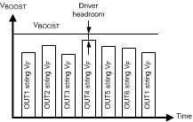
LP8556 supports a mode of output voltage control called Adaptive Boost Control mode. In this mode, the voltage at the LED pins is periodically monitored by the control loop and adaptively adjusted to the optimum value based on the comparator thresholds set using LED DRIVER_HEADROOM, LED_COMP_HYST, BOOST_STEP_UP, BOOST_STEP_DOWN fields in the EPROM. Settings under LED DRIVER_HEADROOM along with LED_COMP_HYST fields determine optimum boost voltage for a given condition. Boost voltage is raised if the voltage measured at any of the LED strings falls below the threshold setting determined with LED DRIVER_HEADROOM field. Likewise, boost voltage is lowered if the voltage measured at any of the LED strings is above the combined setting determined under LED DRIVER_HEADROOM and LED_COMP_HYST fields. LED_COMP_HYST field serves to fine tune the headroom voltage for a given peak LED current. The boost voltage up/down step size can be controlled with the BOOST_STEP_UP and BOOST_STEP_DN fields.
The initial boost voltage is configured with the VBOOST field. This field also sets the minimum boost voltage. The VBOOST_MAX field sets the maximum boost voltage. When an LED pin is open, the monitored voltage never has enough headroom, and the adaptive mode control loop keeps raising the boost voltage. The VBOOST_MAX field allows the boost voltage to be limited to stay under the voltage rating of the external components.
NOTE
Only LED strings that are enabled are monitored and PS_MODE field determines which LED strings are enabled.
The adaptive mode is selected using ADAPTIVE bit set to 1 (CFGA EPROM Register) and is the recommended mode of boost control.
 Figure 5. Boost Adaptive Control Principle