JAJSEF5L July   2012  – May 2019 LP8556

PRODUCTION DATA.  

  1. 特長
  2. アプリケーション
    1.     概略回路図
  3. 概要
  4. 改訂履歴
  5. Device Options
  6. Pin Configuration and Functions
    1.     Pin Functions
  7. Specifications
    1. 7.1  Absolute Maximum Ratings
    2. 7.2  ESD Ratings
    3. 7.3  Recommended Operating Conditions
    4. 7.4  Thermal Information
    5. 7.5  Electrical Characteristics
    6. 7.6  Electrical Characteristics — Boost Converter
    7. 7.7  Electrical Characteristics — LED Driver
    8. 7.8  Electrical Characteristics — PWM Interface
    9. 7.9  Electrical Characteristics — Logic Interface
    10. 7.10 I2C Serial Bus Timing Parameters (SDA, SCL)
    11. 7.11 Typical Characteristics
  8. Detailed Description
    1. 8.1 Overview
    2. 8.2 Functional Block Diagram
    3. 8.3 Feature Description
      1. 8.3.1 Boost Converter
        1. 8.3.1.1 Boost Converter Operation
        2. 8.3.1.2 Setting Boost Switching Frequency
        3. 8.3.1.3 Output Voltage Control
          1. 8.3.1.3.1 Adaptive Control
          2. 8.3.1.3.2 Manual Control
        4. 8.3.1.4 EMI Reduction
      2. 8.3.2 Brightness Control
        1. 8.3.2.1  BRT_MODE = 00
        2. 8.3.2.2  BRT_MODE = 01
        3. 8.3.2.3  BRT_MODE = 10
        4. 8.3.2.4  BRT_MODE = 11
        5. 8.3.2.5  Output Dimming Schemes
          1. 8.3.2.5.1 PWM Control
          2. 8.3.2.5.2 Pure Current Control
          3. 8.3.2.5.3 Adaptive Control
        6. 8.3.2.6  Setting Full-Scale LED Current
        7. 8.3.2.7  Setting PWM Dimming Frequency
        8. 8.3.2.8  Phase Shift PWM Scheme
        9. 8.3.2.9  Slope and Advanced Slope
        10. 8.3.2.10 Dithering
      3. 8.3.3 Fault Detection
        1. 8.3.3.1 LED Fault Detection
          1. 8.3.3.1.1 Open Detect
          2. 8.3.3.1.2 Short Detect
        2. 8.3.3.2 Undervoltage Detection
        3. 8.3.3.3 Overcurrent Protection
        4. 8.3.3.4 Thermal Shutdown
    4. 8.4 Device Functional Modes
      1. 8.4.1 Shutdown Mode
      2. 8.4.2 Active Mode
    5. 8.5 Programming
      1. 8.5.1 I2C-Compatible Serial Bus Interface
        1. 8.5.1.1 Interface Bus Overview
        2. 8.5.1.2 Data Transactions
        3. 8.5.1.3 Acknowledge Cycle
        4. 8.5.1.4 Acknowledge After Every Byte Rule
        5. 8.5.1.5 Addressing Transfer Formats
        6. 8.5.1.6 Control Register Write Cycle
        7. 8.5.1.7 Control Register Read Cycle
        8. 8.5.1.8 Register Read and Write Detail
    6. 8.6 Register Maps
      1. 8.6.1 Register Bit Explanations
        1. 8.6.1.1 Brightness Control
        2. 8.6.1.2 Device Control
        3. 8.6.1.3 Status
        4. 8.6.1.4 Direct Control
        5. 8.6.1.5 LED String Enable
      2. 8.6.2 EPROM Bit Explanations
        1. 8.6.2.1  LP8556TM (DSBGA) Configurations and Pre-Configured EPROM Settings
        2. 8.6.2.2  LP8556TM (DSBGA) Configurations and Pre-configured EPROM Settings Continued
        3. 8.6.2.3  LP8556SQ (WQFN) Configurations and Pre-configured EPROM Settings
        4. 8.6.2.4  CFG98
        5. 8.6.2.5  CFG9E
        6. 8.6.2.6  CFG0
        7. 8.6.2.7  CFG1
        8. 8.6.2.8  CFG2
        9. 8.6.2.9  CFG3
        10. 8.6.2.10 CFG4
        11. 8.6.2.11 CFG5
        12. 8.6.2.12 CFG6
        13. 8.6.2.13 CFG7
        14. 8.6.2.14 CFG9
        15. 8.6.2.15 CFGA
        16. 8.6.2.16 CFGE
        17. 8.6.2.17 CFGF
  9. Application and Implementation
    1. 9.1 Application Information
      1. 9.1.1 Using LP8556 With I2C Host
        1. 9.1.1.1 Setting Boost Switching and PWM Dimming Frequencies
        2. 9.1.1.2 Setting Full-Scale LED Current
      2. 9.1.2 Using LP8556 With Configuration Resistors and IO Pins
        1. 9.1.2.1 Setting Boost Switching and PWM Dimming Frequencies
        2. 9.1.2.2 Setting Full-Scale LED Current
    2. 9.2 Typical Application
      1. 9.2.1 Design Requirements
      2. 9.2.2 Detailed Design Procedure
        1. 9.2.2.1 Recommended Inductance for the Boost Power Stage
        2. 9.2.2.2 Recommended Capacitances for the Boost and LDO Power Stages
      3. 9.2.3 Application Curves
  10. 10Power Supply Recommendations
  11. 11Layout
    1. 11.1 Layout Guidelines
    2. 11.2 Layout Examples
  12. 12デバイスおよびドキュメントのサポート
    1. 12.1 ドキュメントの更新通知を受け取る方法
    2. 12.2 コミュニティ・リソース
    3. 12.3 商標
    4. 12.4 静電気放電に関する注意事項
    5. 12.5 Glossary
  13. 13メカニカル、パッケージ、および注文情報

Adaptive Control

Adaptive dimming control combines PWM Control and Pure Current Control dimming methods. With the adaptive dimming, it is possible to achieve better optical efficiency from the LEDs compared to pure PWM control while still achieving smooth and accurate control at low brightness levels. Current resolution in this mode is 12 bits. Switch point from Current to PWM control can be set with the PWM_TO_I_THRESHOLD EPROM field from 0% to 100% of the brightness range to get good compromise between good matching of the LEDs brightness/white point at low brightness and good optical efficiency.

PWM frequency is set either using an external set Resistor (RFSET) or using the PWM_FREQ EPROM bits. The maximum LED current is set either by using an external set Resistor (RISET), CURRENT, and CURRENT_MAX EPROM bits. Or the maximum LED current may be set using the CURRENT and CURRENT_MAX EPROM bits.
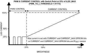
LP8556 30162604.gifFigure 10. Adaptive Output Dimming Scheme