JAJSEF5L July 2012 – May 2019 LP8556
PRODUCTION DATA.
- 1 特長
- 2 アプリケーション
- 3 概要
- 4 改訂履歴
- 5 Device Options
- 6 Pin Configuration and Functions
-
7 Specifications
- 7.1 Absolute Maximum Ratings
- 7.2 ESD Ratings
- 7.3 Recommended Operating Conditions
- 7.4 Thermal Information
- 7.5 Electrical Characteristics
- 7.6 Electrical Characteristics — Boost Converter
- 7.7 Electrical Characteristics — LED Driver
- 7.8 Electrical Characteristics — PWM Interface
- 7.9 Electrical Characteristics — Logic Interface
- 7.10 I2C Serial Bus Timing Parameters (SDA, SCL)
- 7.11 Typical Characteristics
-
8 Detailed Description
- 8.1 Overview
- 8.2 Functional Block Diagram
- 8.3
Feature Description
- 8.3.1 Boost Converter
- 8.3.2 Brightness Control
- 8.3.3 Fault Detection
- 8.4 Device Functional Modes
- 8.5 Programming
- 8.6
Register Maps
- 8.6.1 Register Bit Explanations
- 8.6.2
EPROM Bit Explanations
- 8.6.2.1 LP8556TM (DSBGA) Configurations and Pre-Configured EPROM Settings
- 8.6.2.2 LP8556TM (DSBGA) Configurations and Pre-configured EPROM Settings Continued
- 8.6.2.3 LP8556SQ (WQFN) Configurations and Pre-configured EPROM Settings
- 8.6.2.4 CFG98
- 8.6.2.5 CFG9E
- 8.6.2.6 CFG0
- 8.6.2.7 CFG1
- 8.6.2.8 CFG2
- 8.6.2.9 CFG3
- 8.6.2.10 CFG4
- 8.6.2.11 CFG5
- 8.6.2.12 CFG6
- 8.6.2.13 CFG7
- 8.6.2.14 CFG9
- 8.6.2.15 CFGA
- 8.6.2.16 CFGE
- 8.6.2.17 CFGF
- 9 Application and Implementation
- 10Power Supply Recommendations
- 11Layout
- 12デバイスおよびドキュメントのサポート
- 13メカニカル、パッケージ、および注文情報
8.3.2.8 Phase Shift PWM Scheme
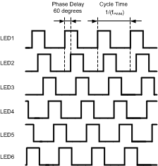
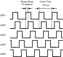
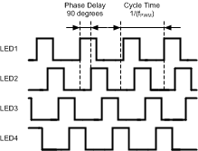
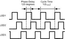
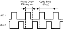
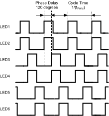
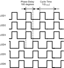
Phase shift PWM scheme allows delaying the time when each LED driver is active. When the LED drivers are not activated simultaneously, the peak load current from the boost output is greatly decreased. This reduces the ripple seen on the boost output and allows smaller output capacitors. Reduced ripple also reduces the output ceramic capacitor audible ringing. PSPWM scheme also increases the load frequency seen on the boost output six times and therefore transfers the possible audible noise to the frequencies outside of the audible range.
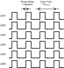
Description of the PSPWM mode is seen inTable 6. PSPWM mode is set with <PS_MODE[2:0]> bits.
Table 6. LED String Configuration
| PS_MODE[2:0] | WAVEFORMS | CONNECTION |
|---|---|---|
| 000 |
 |
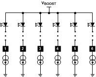 |
| 6 LED strings with 60 degree phase shift. One driver for each LED string. | ||
| 001 |
 |
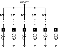 |
| 5 LED strings with 72 degree phase shift. One driver for each LED string.
(Driver #6 not used). |
||
| 010 |
 |
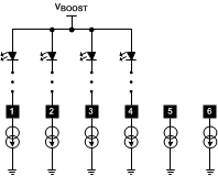 |
| 4 LED strings with 90 degree phase shift. One driver for each LED string.
(Drivers #5 and #6 not used). |
||
| 011 |
 |
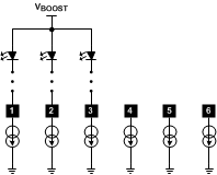 |
| 3 LED strings with 120 degree phase shift. One driver for each LED string.
(Drivers #4, #5 and #6 not used). |
||
| 100 |
 |
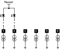 |
| 2 LED strings with 180 degree phase shift. One driver for each LED string.
(Drivers #3, #4, #5 and #6 not used). |
||
| 101 |
 |
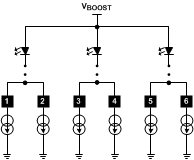 |
| 3 LED strings with 120 degree phase shift. Two drivers for each LED string.
(Drivers 1&2, 3&4 and 5&6 are tied and with the same phase). |
||
| 110 |
 |
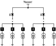 |
| 2 LED strings with 180 degree phase shift. Three divers for each LED string.
(Drivers 1&2&3 and 4&5&6 are tied and with the same phase). |
||
| 111 |
 |
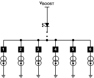 |
| 1 LED string driven by all six drivers.
(All drivers are tied and with the same phase). |
||