JAJSEF5L July 2012 – May 2019 LP8556
PRODUCTION DATA.
- 1 特長
- 2 アプリケーション
- 3 概要
- 4 改訂履歴
- 5 Device Options
- 6 Pin Configuration and Functions
-
7 Specifications
- 7.1 Absolute Maximum Ratings
- 7.2 ESD Ratings
- 7.3 Recommended Operating Conditions
- 7.4 Thermal Information
- 7.5 Electrical Characteristics
- 7.6 Electrical Characteristics — Boost Converter
- 7.7 Electrical Characteristics — LED Driver
- 7.8 Electrical Characteristics — PWM Interface
- 7.9 Electrical Characteristics — Logic Interface
- 7.10 I2C Serial Bus Timing Parameters (SDA, SCL)
- 7.11 Typical Characteristics
-
8 Detailed Description
- 8.1 Overview
- 8.2 Functional Block Diagram
- 8.3
Feature Description
- 8.3.1 Boost Converter
- 8.3.2 Brightness Control
- 8.3.3 Fault Detection
- 8.4 Device Functional Modes
- 8.5 Programming
- 8.6
Register Maps
- 8.6.1 Register Bit Explanations
- 8.6.2
EPROM Bit Explanations
- 8.6.2.1 LP8556TM (DSBGA) Configurations and Pre-Configured EPROM Settings
- 8.6.2.2 LP8556TM (DSBGA) Configurations and Pre-configured EPROM Settings Continued
- 8.6.2.3 LP8556SQ (WQFN) Configurations and Pre-configured EPROM Settings
- 8.6.2.4 CFG98
- 8.6.2.5 CFG9E
- 8.6.2.6 CFG0
- 8.6.2.7 CFG1
- 8.6.2.8 CFG2
- 8.6.2.9 CFG3
- 8.6.2.10 CFG4
- 8.6.2.11 CFG5
- 8.6.2.12 CFG6
- 8.6.2.13 CFG7
- 8.6.2.14 CFG9
- 8.6.2.15 CFGA
- 8.6.2.16 CFGE
- 8.6.2.17 CFGF
- 9 Application and Implementation
- 10Power Supply Recommendations
- 11Layout
- 12デバイスおよびドキュメントのサポート
- 13メカニカル、パッケージ、および注文情報
8.5.1.2 Data Transactions
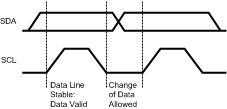
One data bit is transferred during each clock pulse. Data is sampled during the high state of the serial clock SCL. Consequently, throughout the clock’s high period, the data should remain stable. Any changes on the SDA line during the high state of the SCL and in the middle of a transaction, aborts the current transaction. New data should be sent during the low SCL state. This protocol permits a single data line to transfer both command/control information and data using the synchronous serial clock.
 Figure 13. Bit Transfer
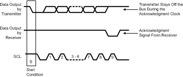
 Each data transaction is composed of a Start Condition, a number of byte transfers (set by the software) and a Stop Condition to terminate the transaction. Every byte written to the SDA bus must be 8 bits long and is transferred with the most significant bit first. After each byte, an Acknowledge signal must follow. The following sections provide further details of this process.
 Figure 14. Start and Stop
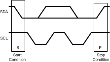
 The Master device on the bus always generates the Start and Stop Conditions (control codes). After a Start Condition is generated, the bus is considered busy and it retains this status until a certain time after a Stop Condition is generated. A high-to-low transition of the data line (SDA) while the clock (SCL) is high indicates a Start Condition. A low-to-high transition of the SDA line while the SCL is high indicates a Stop Condition.
 Figure 15. Start and Stop Conditions
 In addition to the first Start Condition, a repeated Start Condition can be generated in the middle of a transaction. This allows another device to be accessed, or a register read cycle.