JAJSEJ4C January 2018 – July 2018 TPSM84209
PRODUCTION DATA.
- 1 特長
- 2 アプリケーション
- 3 概要
- 4 改訂履歴
- 5 Pin Configuration and Functions
- 6 Specifications
-
7 Detailed Description
- 7.1 Overview
- 7.2 Functional Block Diagram
- 7.3
Feature Description
- 7.3.1 Adjusting the Output Voltage
- 7.3.2 Input Capacitor Selection
- 7.3.3 Undervoltage Lockout (UVLO)
- 7.3.4 Output Capacitor Selection
- 7.3.5 Feed-Forward Capacitor
- 7.3.6 Operating Range
- 7.3.7 Output Current Rating
- 7.3.8 Enable (EN)
- 7.3.9 Internal Soft Start
- 7.3.10 Safe Start-Up Into Prebiased Outputs
- 7.3.11 Light Load Efficiency / Eco-Mode
- 7.3.12 Voltage Dropout
- 7.3.13 Overcurrent Protection
- 7.3.14 Output Overvoltage Protection (OVP)
- 7.3.15 Thermal Performance
- 7.3.16 Thermal Shutdown
- 7.4 Device Functional Modes
- 8 Application and Implementation
- 9 Power Supply Recommendations
- 10Layout
- 11デバイスおよびドキュメントのサポート
- 12メカニカル、パッケージ、および注文情報
7.3.5 Feed-Forward Capacitor
The TPSM84209 is internally compensated to be stable over the operating range of the device. However, depending on the output voltage and amount of output capacitance, an additional feed-forward capacitor, CFF, may be added for optimum performance. Adding additional output capacitance above the minimum reduces the output voltage ripple of the device. However, adding additional output capacitance also reduces the cross-over frequency of the device, slowing the response to load transients. Adding a feed-forward capacitor when adding more output capacitance helps to restore cross-over frequency of the device, restoring the transient response.
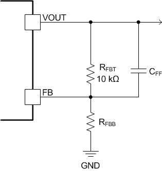
The external feed-forward capacitor must be placed in parallel with the top resistor divider, RFBT. The placement of CFF is shown in Figure 19. Table 6 lists the required CFF values for different amounts of output capacitance. For output voltages < 2.5 V, it is not recommended to add a CFF capacitor.
 Figure 19. Feed-Forward Capacitor
 Table 6. CFF Values(1)
| VOUT RANGE (V) | Amount of COUT | ||||
|---|---|---|---|---|---|
| MIN | MAX | 47 µF (1 x 47 µF) | 94 µF (2 x 47 µF) | 141 µF (3 x 47 µF) | ≥ 188 µF (4 x 47 µF) |
| 2.5 | < 3.3 | Not applicable | CFF = 100 pF | CFF = 220 pF | CFF = 330 pF |
| 3.3 | < 5 | Not applicable | CFF = 100 pF | CFF = 330 pF | CFF = 330 pF |
| 5 | 6 | CFF = 100 pF | CFF = 330 pF | CFF = 330 pF | CFF = 330 pF |