JAJSEM0D February 2018 – April 2024 TUSB1044
PRODUCTION DATA
- 1
- 1 特長
- 2 アプリケーション
- 3 概要
- 4 Pin Configuration and Functions
- 5 Specifications
- 6 Detailed Description
- 7 Application and Implementation
- 8 Device and Documentation Support
- 9 Revision History
- 10Mechanical, Packaging, and Orderable Information
5.7 Timing Requirements
| MIN | NOM | MAX | UNIT | ||
|---|---|---|---|---|---|
| I2C Timing | |||||
| fSCL | I2C clock frequency | 1 | MHz | ||
| tBUF | Bus free time between START and STOP conditions | 0.5 | µs | ||
| tHDSTA | Hold time after repeated START condition. After this period, the first clock pulse is generated | 0.26 | µs | ||
| tLOW | Low period of the I2C clock | 0.5 | µs | ||
| tHIGH | High period of the I2C clock | 0.26 | µs | ||
| tSUSTA | Setup time for a repeated START condition | 0.26 | µs | ||
| tHDDAT | Data hold time | 0 | µs | ||
| tSUDAT | Data setup time | 50 | ns | ||
| tR | Rise time of both SDA and SCL signals | 120 | ns | ||
| tF | Fall time of both SDA and SCL signals | 20 × (VI2C/5.5 V) | 120 | ns | |
| tSUSTO | Setup time for STOP condition | 0.26 | µs | ||
| CBUS | Capacitive load for each bus line | 100 | pF | ||
| HPDIN and CTL1 | |||||
| tCTL1_DEBOUNCE | CTL1 and HPDIN debounce time when transitioning from H to L. DP lanes will be disabled if low is greater than min value. | 2.5 | ms | ||
| USB3.1 and DisplayPort mode transition requirement GPIO mode | |||||
| tGP_USB_4DP | Min overlap of CTL0 and CTL1 when transitioning from USB 3.1 only mode to 4-Lane DisplayPort mode or vice versa. Refer to Figure 5-2 | 4 | µs | ||
| Power-on timings | |||||
| td_pg | VCC(MIN) to Internal power good asserted high. Refer to Figure 5-8 | 500 | µs | ||
| tcfg_su | CFG pins setup. Refer to Figure 5-8 | 350 | µs | ||
| tcfg_hd | CFG pin hold. Refer to Figure 5-8 | 10 | µs | ||
| tctl_db | CTL[1:0] and FLIP pin debounce. Refer to Figure 5-8 | 16 | ms | ||
| tVCC_RAMP | VCC supply ramp requirement. Refer to Figure 5-8 | 0.1 | 100 | ms | |
 Figure 5-1 I2C Timing Diagram Definitions
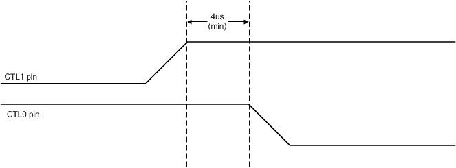 Figure 5-2 USB3.1 to 4-Lane DisplayPort in GPIO Mode
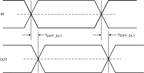 Figure 5-3 Propagation Delay
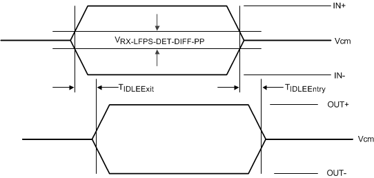 Figure 5-4 Electrical Idle Mode Exit and Entry Delay
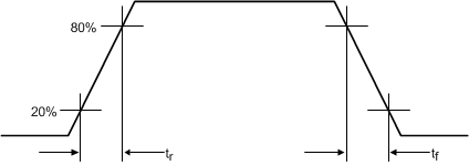 Figure 5-5 Output Rise and Fall Times
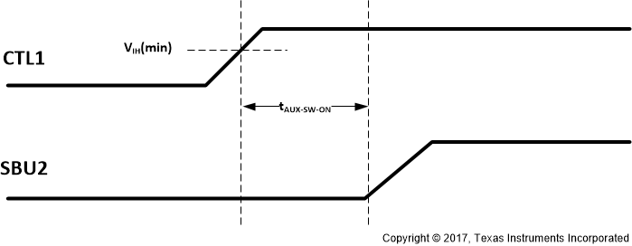 Figure 5-6 AUX to SBU Switch ON Timing Diagram
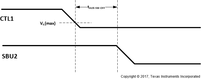 Figure 5-7 AUX to SBU Switch OFF Timing Diagram
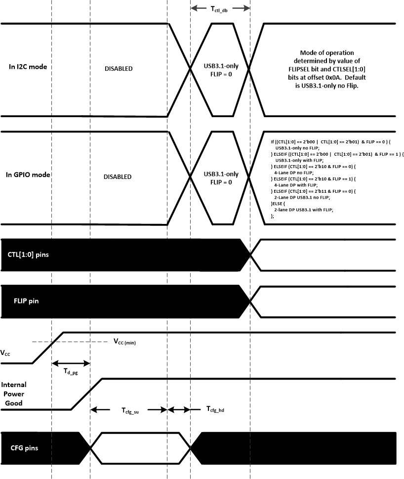 Figure 5-8 Power-Up Timing Diagram