JAJSEO7I October 2008 – December 2017 TPS23754 , TPS23754-1 , TPS23756
PRODUCTION DATA.
- 1 特長
- 2 アプリケーション
- 3 概要
- 4 改訂履歴
- 5 概要(続き)
- 6 Pin Configuration and Functions
- 7 Specifications
-
8 Detailed Description
- 8.1 Overview
- 8.2 Functional Block Diagram
- 8.3 Feature Description
- 8.4
Device Functional Modes
- 8.4.1
PoE Overview
- 8.4.1.1 Threshold Voltages
- 8.4.1.2 PoE Start-Up Sequence
- 8.4.1.3 Detection
- 8.4.1.4 Hardware Classification
- 8.4.1.5 Inrush and Start-Up
- 8.4.1.6 Maintain Power Signature
- 8.4.1.7 Start-Up and Converter Operation
- 8.4.1.8 PD Hotswap Operation
- 8.4.1.9 Converter Controller Features
- 8.4.1.10 Bootstrap Topology
- 8.4.1.11 Current Slope Compensation and Current Limit
- 8.4.1.12 Blanking – RBLNK
- 8.4.1.13 Dead Time
- 8.4.1.14 FRS and Synchronization
- 8.4.1.15 T2P, Start-Up, and Power Management
- 8.4.1.16 Thermal Shutdown
- 8.4.1.17 Adapter ORing
- 8.4.1.18 PPD ORing Features
- 8.4.1.19 Using DEN to Disable PoE
- 8.4.1.20 ORing Challenges
- 8.4.1
PoE Overview
-
9 Application and Implementation
- 9.1 Application Information
- 9.2
Typical Application
- 9.2.1 Design Requirements
- 9.2.2
Detailed Design Procedure
- 9.2.2.1 Input Bridges and Schottky Diodes
- 9.2.2.2 Protection, D1
- 9.2.2.3 Capacitor, C1
- 9.2.2.4 Detection Resistor, RDEN
- 9.2.2.5 Classification Resistor, RCLS
- 9.2.2.6 Dead Time Resistor, RDT
- 9.2.2.7 Switching Transformer Considerations and RVC
- 9.2.2.8 Special Switching MOSFET Considerations
- 9.2.2.9 Thermal Considerations and OTSD
- 9.2.2.10 APD Pin Divider Network, RAPD1, RAPD2
- 9.2.2.11 PPD Pin Divider Network, RPPD1, RPPD2
- 9.2.2.12 Setting Frequency (RFRS) and Synchronization
- 9.2.2.13 Current Slope Compensation
- 9.2.2.14 Blanking Period, RBLNK
- 9.2.2.15 Estimating Bias Supply Requirements and CVC
- 9.2.2.16 T2P Pin Interface
- 9.2.2.17 Advanced ORing Techniques
- 9.2.2.18 Soft Start
- 9.2.2.19 Frequency Dithering for Conducted Emissions Control
- 9.2.3 Application Curves
- 10Power Supply Recommendations
- 11Layout
- 12デバイスおよびドキュメントのサポート
- 13メカニカル、パッケージ、および注文情報
9.2.2.17 Advanced ORing Techniques
See Advanced Adapter ORing Solutions using the TSP23753, TI document number SLVA306A for ORing applications that also work with the TPS23754 device. The material in sections Adapter ORing and Protection, D1 are important to consider as well. The following applications are unique to the TPS23754 device with the introduction of PPD.
Option 2 ORing with PoE acting as a hot backup is eased by connecting PPD to VDD per Figure 33. This PPD connection enables the class regulator even when APD is high. The R-Zener network (1.8 kΩ – 24 V) is the simplest circuit that will satisfy MPS requirements, keeping the PSE online. This network may be switched out when the APD is not powered with an optocoupler. This works best with a 48-V adapter and the APD-programmed threshold as high as possible. An example of an adapter priority application with smooth switchover between a 48-V adapter and PoE is shown on the right side of Figure 33. DAPD is used to reduce the effective APD hysteresis, allowing the PSE to power the load before VVDD1-VRTN falls too low and causes a hotswap foldback.
 Figure 33. Option 2 PoE Backup ORing
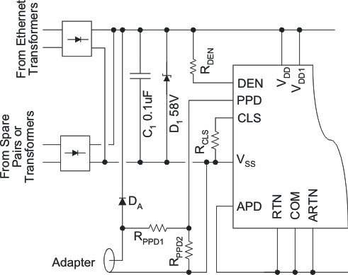
Option 1 ORing of a low voltage adapter (for example, 24 V) is possible by connecting a resistor divider to PPD as in Figure 34. When 1.55 V ≤ VPPD ≤ 8.3 V, the hotswap MOSFET is enabled, T2P is activated, and the class feature is disabled. The hotswap current limit is unaffected, limiting the available power. For example, the maximum input power from a 24-V adapter would be 19.3 W [(24 V – 0.6 V) × 0.825 A].
 Figure 34. Low-Voltage Option 1 ORing