JAJSEO9D December 2017 – August 2020 LMZM33602
PRODUCTION DATA
- 1特長
- 2アプリケーション
- 3概要
- 4Revision History
- 5Pin Configuration and Functions
- 6Specifications
-
7Detailed Description
- 7.1 Overview
- 7.2 Functional Block Diagram
- 7.3
Feature Description
- 7.3.1 Adjusting the Output Voltage
- 7.3.2 Feedforward Capacitor, CFF
- 7.3.3 Voltage Dropout
- 7.3.4 Switching Frequency (RT)
- 7.3.5 Synchronization (SYNC)
- 7.3.6 Input Capacitors
- 7.3.7 Output Capacitors
- 7.3.8 Output On/Off Enable (EN)
- 7.3.9 Programmable Undervoltage Lockout (UVLO)
- 7.3.10 Power Good (PGOOD)
- 7.3.11 Overcurrent Protection (OCP)
- 7.3.12 Thermal Shutdown
- 7.4 Device Functional Modes
- 8Application and Implementation
- 9Device and Documentation Support
7.3.3 Voltage Dropout
Voltage dropout is the difference between the input voltage and output voltage that is required to maintain output voltage regulation while providing the rated output current.
To ensure the LMZM33602 maintains output voltage regulation at the recommended switching frequency, over the operating temperature range, the following requirements apply:
For output voltages ≤ 5 V, the minimum VIN is 4 V or (VOUT + 1.5 V), whichever is greater.
For output voltages > 5 V, the minimum VIN is (1.3 × VOUT).
However, if fixed switching frequency operation is not required, the LMZM33602 operates in a frequency foldback mode when the dropout voltage is less than the recommendations above. Frequency foldback reduces the switching frequency to allow the output voltage to maintain regulation as input voltage decreases. Figure 7-2 through Figure 7-7 show typical dropout voltage and frequency foldback curves for 3.3-V, 5-V, and 12-V outputs at TA = 25°C. (Note: As ambient temperature increases, dropout voltage and frequency foldback occur at higher input voltage.)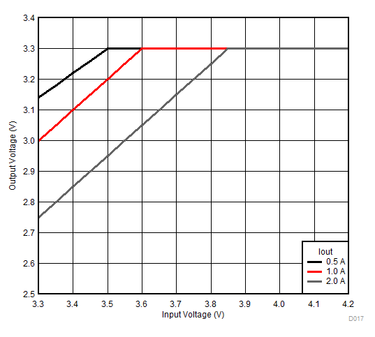
| VOUT = 3.3 V | fSW = 300 kHz |
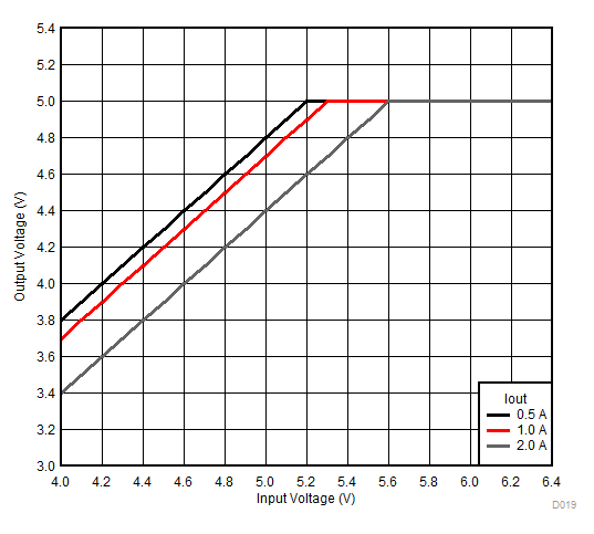
| VOUT = 5 V | fSW = 450 kHz |
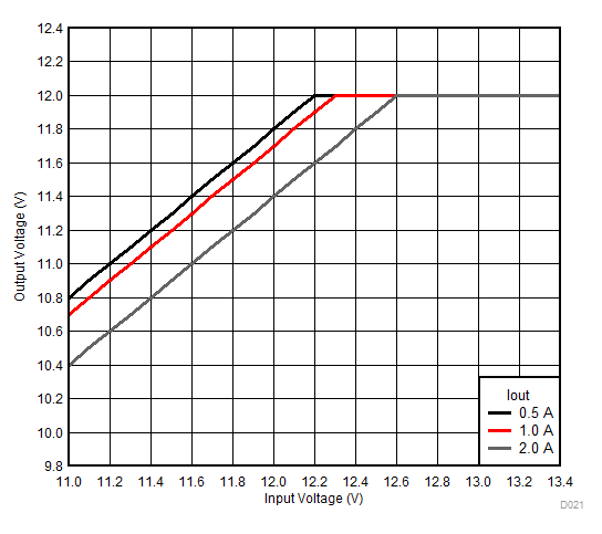
| VOUT = 12 V | fSW = 900 kHz |
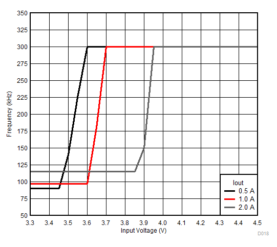
| VOUT = 3.3 V | fSW = 300 kHz |
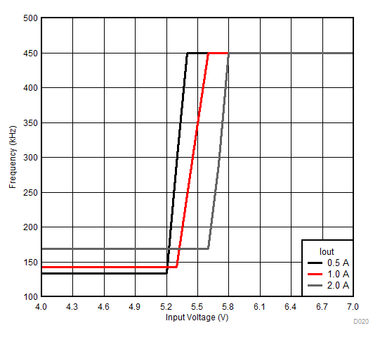
| VOUT = 5 V | fSW = 450 kHz |
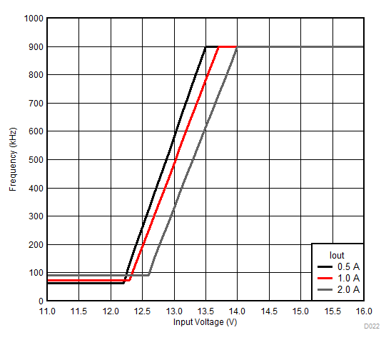
| VOUT = 12 V | fSW = 900 kHz |