JAJSEO9D December 2017 – August 2020 LMZM33602
PRODUCTION DATA
- 1特長
- 2アプリケーション
- 3概要
- 4Revision History
- 5Pin Configuration and Functions
- 6Specifications
-
7Detailed Description
- 7.1 Overview
- 7.2 Functional Block Diagram
- 7.3
Feature Description
- 7.3.1 Adjusting the Output Voltage
- 7.3.2 Feedforward Capacitor, CFF
- 7.3.3 Voltage Dropout
- 7.3.4 Switching Frequency (RT)
- 7.3.5 Synchronization (SYNC)
- 7.3.6 Input Capacitors
- 7.3.7 Output Capacitors
- 7.3.8 Output On/Off Enable (EN)
- 7.3.9 Programmable Undervoltage Lockout (UVLO)
- 7.3.10 Power Good (PGOOD)
- 7.3.11 Overcurrent Protection (OCP)
- 7.3.12 Thermal Shutdown
- 7.4 Device Functional Modes
- 8Application and Implementation
- 9Device and Documentation Support
7.3.9 Programmable Undervoltage Lockout (UVLO)
The LMZM33602 implements internal UVLO circuitry on the VIN pin. The device is disabled when the VIN pin voltage falls below the internal VIN UVLO threshold. The internal VIN UVLO rising threshold is 3.9 V (maximum) with a typical hysteresis of 300 mV.
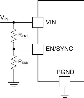
If an application requires a higher UVLO threshold, a resistor divider can be placed on the EN/SYNC pin as shown in Figure 7-13. Table 7-6 lists recommended resistor values for RENT and RENB to adjust the ULVO voltage.
To ensure proper start-up and reduce input current surges, the UVLO threshold must be set to at least (VOUT + 1.5 V) for output voltages ≤ 5 V and at least (1.3 × VOUT) for output voltages > 5 V. TI recommends to set the UVLO threshold to approximately 80% to 85% of the minimum expected input voltage.
 Figure 7-13 Adjustable UVLO
| VIN UVLO (V) | 6.5 | 10 | 15 | 20 | 25 | 30 |
|---|---|---|---|---|---|---|
| RENT (kΩ) | 100 | 100 | 100 | 100 | 100 | 100 |
| RENB (kΩ) | 35.7 | 20.5 | 12.7 | 9.31 | 7.32 | 6.04 |