JAJSEU9B
September 2017 – September 2019
BQ25910
PRODUCTION DATA.
1
特長
2
アプリケーション
3
概要
概略回路図
4
改訂履歴
5
Pin Configuration and Functions
Pin Functions
6
Specifications
6.1
Absolute Maximum Ratings
6.2
ESD Ratings
6.3
Recommended Operating Conditions
6.4
Thermal Information
6.5
Electrical Characteristics
6.6
Timing Requirements
6.7
Typical Characteristics
7
Detailed Description
7.1
Overview
7.2
Functional Block Diagram
7.3
Feature Description
7.3.1
Device Power-On-Reset (POR)
7.3.2
Device Power Up from Battery without Input Source
7.3.3
Device Power Up from Input Source
7.3.4
Power Up REGN LDO
7.3.5
Poor Source Qualification
7.3.6
Converter Power-Up
7.3.7
Three-Level Buck Converter Theory of Operation
7.3.8
Host Mode and Default Mode
7.3.8.1
Host Mode and Default Mode in BQ25910
7.3.9
Battery Charging Management
7.3.9.1
Autonomous Charging Cycle
7.3.10
Master Charger and Parallel Charger Interactions
7.3.11
Battery Charging Profile
7.3.11.1
Charging Termination
7.3.11.2
Differential Battery Voltage Remote Sensing
7.3.11.3
Charging Safety Timer
7.4
Device Functional Modes
7.4.1
Lossless Current Sensing
7.4.2
Dynamic Power Management
7.4.3
Interrupt to Host (INT)
7.4.4
Protections
7.4.4.1
Voltage and Current Monitoring
7.4.4.1.1
Input Over-Voltage (VVBUS_OV)
7.4.4.1.2
Input Under-Voltage (VPOORSRC)
7.4.4.1.3
Flying Capacitor Over- or Under-Voltage Protection (VCFLY_OVP and VCFLY_UVP)
7.4.4.1.4
Over Current Protection
7.4.4.2
Thermal Regulation and Thermal Shutdown
7.4.4.3
Battery Protection
7.4.4.3.1
Battery Over-Voltage Protection (BATOVP)
7.5
Programming
7.5.1
Serial Interface
7.5.2
Data Validity
7.5.3
START and STOP Conditions
7.5.4
Byte Format
7.5.5
Acknowledge (ACK) and Not Acknowledge (NACK)
7.5.6
Slave Address and Data Direction Bit
7.5.7
Single Read and Write
7.5.8
Multi-Read and Multi-Write
7.6
Register Maps
7.6.1
I2C Registers
7.6.1.1
Battery Voltage Regulation Limit Register (Address = 0h) [reset = AAh]
Table 5.
REG00 Register Field Descriptions
7.6.1.2
Charger Current Limit Register (Address = 1h) [reset = 46h]
Table 6.
REG01 Register Field Descriptions
7.6.1.3
Input Voltage Limit Register (Address = 2h) [reset = 04h]
Table 7.
REG02 Register Field Descriptions
7.6.1.4
Input Current Limit Register (Address = 3h) [reset = 13h]
Table 8.
REG03 Register Field Descriptions
7.6.1.5
Reserved Register (Address = 4h) [reset = 03h]
Table 9.
REG04 Register Field Descriptions
7.6.1.6
Charger Control 1 Register (Address = 5h) [reset = 9Dh]
Table 10.
REG05 Register Field Descriptions
7.6.1.7
Charger Control 2 Register (Address = 6h) [reset = 33h]
Table 11.
REG06 Register Field Descriptions
7.6.1.8
INT Status Register (Address = 7h) [reset = X]
Table 12.
REG07 Register Field Descriptions
7.6.1.9
FAULT Status Register (Address = 8h) [reset = X]
Table 13.
REG08 Register Field Descriptions
7.6.1.10
INT Flag Status Register (Address = 9h) [reset = 00h]
Table 14.
REG09 Register Field Descriptions
7.6.1.11
FAULT Flag Register (Address = Ah) [reset = 00h]
Table 15.
REG0A Register Field Descriptions
7.6.1.12
INT Mask Register (Address = Bh) [reset = 00h]
Table 16.
REG0h Register Field Descriptions
7.6.1.13
FAULT Mask Register (Address = Ch) [reset = 00h]
Table 17.
REG0C Register Field Descriptions
7.6.1.14
Part Information Register (Address = Dh) [reset = 0Ah]
Table 18.
REG0D Register Field Descriptions
8
Application and Implementation
8.1
Application Information
8.2
Typical Application
8.2.1
Design Requirements
8.2.2
Detailed Design Procedure
8.2.2.1
External Passive Recommendation
8.2.2.2
Inductor Selection
8.2.2.3
Input Capacitor
8.2.2.4
Flying Capacitor
8.2.2.5
Output Capacitor
8.2.3
Application Curves
9
Power Supply Recommendations
10
Layout
10.1
Layout Guidelines
10.2
Layout Example
11
デバイスおよびドキュメントのサポート
11.1
デバイス・サポート
11.1.1
デベロッパー・ネットワークの製品に関する免責事項
11.1.1.1
デベロッパー・ネットワークの製品に関する免責事項
11.2
ドキュメントの更新通知を受け取る方法
11.3
コミュニティ・リソース
11.4
商標
11.5
静電気放電に関する注意事項
11.6
Glossary
12
メカニカル、パッケージ、および注文情報
10.2
Layout Example
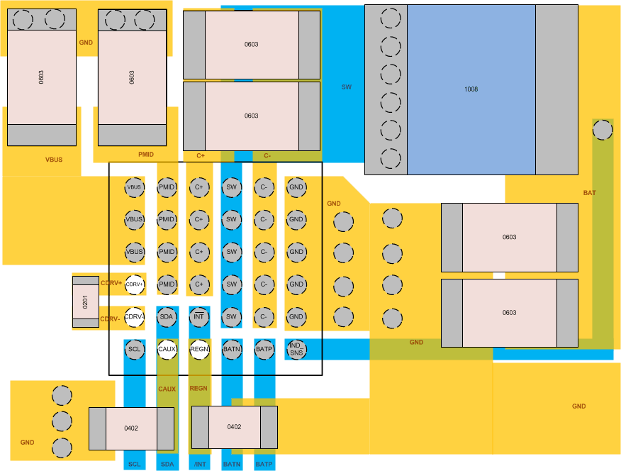
Figure 61.
BQ25910
PCB Layout Example