JAJSF91B April   2018  – March 2020 TLV62568A , TLV62569A

PRODUCTION DATA.  

  1. 特長
  2. アプリケーション
  3. 概要
    1.     Device Images
      1.      sp sp sp代表的なアプリケーションの回路図
      2.      sp sp入力電圧5V時の効率
  4. 改訂履歴
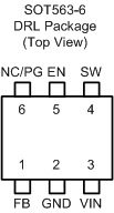
  5. Pin Configuration and Functions
    1.     Pin Functions
  6. Specifications
    1. 6.1 Absolute Maximum Ratings
    2. 6.2 ESD Ratings
    3. 6.3 Recommended Operating Conditions
    4. 6.4 Thermal Information
    5. 6.5 Electrical Characteristics
    6. 6.6 Typical Characteristics
  7. Detailed Description
    1. 7.1 Overview
    2. 7.2 Functional Block Diagrams
    3. 7.3 Feature Description
      1. 7.3.1 100% Duty Cycle Low Dropout Operation
      2. 7.3.2 Soft Startup
      3. 7.3.3 Switch Current Limit
      4. 7.3.4 Under Voltage Lockout
      5. 7.3.5 Thermal Shutdown
    4. 7.4 Device Functional Modes
      1. 7.4.1 Enabling/Disabling the Device
      2. 7.4.2 Power Good
  8. Application and Implementation
    1. 8.1 Application Information
    2. 8.2 Typical Application
      1. 8.2.1 Design Requirements
      2. 8.2.2 Detailed Design Procedure
        1. 8.2.2.1 Custom Design With WEBENCH® Tools
        2. 8.2.2.2 Setting the Output Voltage
        3. 8.2.2.3 Output Filter Design
        4. 8.2.2.4 Inductor Selection
        5. 8.2.2.5 Input and Output Capacitor Selection
      3. 8.2.3 Application Performance Curves
  9. Power Supply Recommendations
  10. 10Layout
    1. 10.1 Layout Guidelines
    2. 10.2 Layout Example
    3. 10.3 Thermal Considerations
  11. 11デバイスおよびドキュメントのサポート
    1. 11.1 デバイス・サポート
      1. 11.1.1 デベロッパー・ネットワークの製品に関する免責事項
      2. 11.1.2 開発サポート
        1. 11.1.2.1 WEBENCH®ツールによるカスタム設計
    2. 11.2 ドキュメントのサポート
      1. 11.2.1 関連資料
    3. 11.3 ドキュメントの更新通知を受け取る方法
    4. 11.4 サポート・リソース
    5. 11.5 商標
    6. 11.6 静電気放電に関する注意事項
    7. 11.7 Glossary
  12. 12メカニカル、パッケージ、および注文情報

Pin Configuration and Functions

TLV62568A TLV62569A Pinout_TLV62569A.gif

Pin Functions

NAME SOT563-6 I/O/PWR DESCRIPTION
PIN NUMBER
FB 1 I Feedback pin for the internal control loop. Connect this pin to an external feedback divider.
GND 2 PWR Ground pin.
VIN 3 PWR Power supply voltage input.
SW 4 PWR Switch pin connected to the internal FET switches and inductor terminal. Connect the inductor of the output filter to this pin.
EN 5 I Device enable logic input. Logic high enables the device, logic low disables the device and turns it into shutdown. Do not leave floating.
PG 6 O Power good open drain output pin for TLV62569APDRL. The pull-up resistor should not be connected to any voltage higher than 5.5V. If it's not used, leave the pin floating.
NC 6 - No connection pin for TLV62569ADRL. The pin can be connected to the output or the ground for enhancing thermal performance. Or leave it floating.