JAJSFE6I July 2009 – May 2018 TPS65070 , TPS65072 , TPS65073 , TPS650731 , TPS650732
UNLESS OTHERWISE NOTED, this document contains PRODUCTION DATA.
- 1 特長
- 2 アプリケーション
- 3 概要
- 4 改訂履歴
- 5 概要(続き)
- 6 Device Options
- 7 Pin Configuration and Functions
-
8 Specifications
- 8.1 Absolute Maximum Ratings
- 8.2 ESD Ratings
- 8.3 Recommended Operating Conditions
- 8.4 Thermal Information
- 8.5 Electrical Characteristics
- 8.6 Electrical Characteristics - DCDC1 Converter
- 8.7 Electrical Characteristics - DCDC2 Converter
- 8.8 Electrical Characteristics - DCDC3 Converter
- 8.9 Electrical Characteristics - VLDO1 and VLDO2 Low Dropout Regulators
- 8.10 Electrical Characteristics - wLED Boost Converter
- 8.11 Electrical Characteristics - Reset, PB_IN, PB_OUT, PGood, Power_on, INT, EN_EXTLDO, EN_wLED
- 8.12 Electrical Characteristics - ADC Converter
- 8.13 Electrical Characteristics - Touch Screen Interface
- 8.14 Electrical Characteristics - Power Path
- 8.15 Electrical Characteristics - Battery Charger
- 8.16 Timing Requirements
- 8.17 Dissipation Ratings
- 8.18 Typical Characteristics
- 9 Parameter Measurement Information
-
10Detailed Description
- 10.1 Overview
- 10.2 Functional Block Diagram
- 10.3
Feature Description
- 10.3.1 Battery Charger and Power Path
- 10.3.2 Power Down
- 10.3.3 Power-On Reset
- 10.3.4 Power-Path Management
- 10.3.5 Battery Charging
- 10.3.6 Battery Pack Temperature Monitoring
- 10.3.7 Battery Charger State Diagram
- 10.3.8 DC-DC Converters and LDOs
- 10.3.9 Power Save Mode
- 10.3.10 Short-Circuit Protection
- 10.3.11 Enable
- 10.3.12 Short-Circuit Protection
- 10.3.13 Thermal Shutdown
- 10.4 Device Functional Modes
- 10.5 Programming
- 10.6
Register Maps
- 10.6.1 PPATH1. Register Address: 01h
- 10.6.2 INT. Register Address: 02h
- 10.6.3 CHGCONFIG0. Register Address: 03h
- 10.6.4 CHGCONFIG1. Register Address: 04h
- 10.6.5 CHGCONFIG2. Register Address: 05h
- 10.6.6 CHGCONFIG3. Register Address: 06h
- 10.6.7 ADCONFIG. Register Address: 07h
- 10.6.8 TSCMODE. Register Address: 08h
- 10.6.9 ADRESULT_1. Register Address: 09h
- 10.6.10 ADRESULT_2. Register Address: 0Ah
- 10.6.11 PGOOD. Register Address: 0Bh
- 10.6.12 PGOODMASK. Register Address: 0Ch
- 10.6.13 CON_CTRL1. Register Address: 0Dh
- 10.6.14 CON_CTRL2. Register Address: 0Eh
- 10.6.15 CON_CTRL3. Register Address: 0Fh
- 10.6.16 DEFDCDC1. Register Address: 10h
- 10.6.17 DEFDCDC2_LOW. Register Address: 11h
- 10.6.18 DEFDCDC2_HIGH. Register Address: 12h
- 10.6.19 DEFDCDC3_LOW. Register Address: 13h
- 10.6.20 DEFDCDC3_HIGH. Register Address: 14h
- 10.6.21 DEFSLEW. Register Address: 15h
- 10.6.22 LDO_CTRL1. Register Address: 16h
- 10.6.23 DEFLDO2. Register Address: 17h
- 10.6.24 WLED_CTRL1. Register Address: 18h
- 10.6.25 WLED_CTRL2. Register Address: 19h
-
11Application and Implementation
- 11.1 Application Information
- 11.2
Typical Applications
- 11.2.1 General PMIC Application
- 11.2.2 Powering OMAP-L138
- 11.2.3 Powering Atlas IV
- 11.2.4 OMAP35xx (Supporting SYS-OFF Mode)
- 11.2.5 TPS650731 for OMAP35xx
- 11.2.6 Powering AM3505 Using TPS650732
- 12Power Supply Recommendations
- 13Layout
- 14デバイスおよびドキュメントのサポート
- 15メカニカル、パッケージ、および注文情報
8.18 Typical Characteristics
Table 1. Table of Graphs
| FIGURE | |||
|---|---|---|---|
| Efficiency DCDC1 vs Load current / PWM mode | VO = 3.3 V; VI = 3 V, 3.6 V, 4.2 V, 5 V | Figure 2 | |
| Efficiency DCDC1 vs Load current / PFM mode | VO = 3.3 V; VI = 3 V, 3.6 V, 4.2 V, 5 V | Figure 3 | |
| Efficiency DCDC2 vs Load current / PWM mode up to 1.5A | VO = 2.5 V; VI = 3 V, 3.6 V, 4.2 V, 5 V | Figure 4 | |
| Efficiency DCDC2 vs Load current / PFM mode up to 1.5A | VO = 2.5 V; VI = 3 V, 3.6 V, 4.2 V, 5 V | Figure 5 | |
| Efficiency DCDC2 vs Load current / PWM mode up to 1.5A | VO = 1.8 V; VI = 3 V, 3.6 V, 4.2 V, 5 V | Figure 6 | |
| Efficiency DCDC2 vs Load current / PFM mode up to 1.5A | VO = 1.8 V; VI = 3 V, 3.6 V, 4.2 V, 5 V | Figure 7 | |
| Efficiency DCDC3 vs Load current / PWM mode up to 1.5A | VO = 1.2 V; VI = 3 V, 3.6 V, 4.2 V, 5 V | Figure 8 | |
| Efficiency DCDC3 vs Load current / PFM mode up to 1.5A | VO = 1.2 V; VI = 3 V, 3.6 V, 4.2 V, 5 V | Figure 9 | |
| Efficiency DCDC3 vs Load current / PWM mode up to 1.5A | VO = 1 V; VI = 3 V, 3.6 V, 4.2 V, 5 V | Figure 10 | |
| Efficiency DCDC3 vs Load current / PFM mode up to 1.5A | VO = 1 V; VI = 3 V, 3.6 V, 4.2 V, 5 V | Figure 11 | |
| Load transient response converter 1 | Scope plot; IO= 60 mA to 540 mA; VO = 3.3 V; VI = 3.6 V | Figure 12 | |
| Load transient response converter 2 | Scope plot; IO= 150 mA to 1350 mA; VO = 1.8 V; VI = 3.6 V | Figure 13 | |
| Load transient response converter 3 | Scope plot; IO= 150 mA to 1350 mA; VO = 1.2 V; VI = 3.6 V | Figure 14 | |
| Line transient response converter 1 | Scope plot; VO= 3.3; VI = 3.6 V to 5 V to 3.6 V; IO= 600 mA | Figure 15 | |
| Line transient response converter 2 | Scope plot; VO= 1.8; VI = 3.6 V to 5 V to 3.6 V; IO = 600 mA | Figure 16 | |
| Line transient response converter 3 | Scope plot; VO = 1.2 V; VI=3.6 V to 5 V to 3.6 V; IO = 600 mA | Figure 17 | |
| Output voltage ripple and inductor current converter 2;
PWM Mode |
Scope plot; VI = 3.6 V; VO=1.8 V; IO = 10 mA | Figure 18 | |
| Output voltage ripple and inductor current converter 2;
PFM Mode |
Scope plot; VI = 3.6 V; VO=1.8 V; IO = 10 mA | Figure 19 | |
| Startup DCDC1, DCDC2 and DCDC3, LDO1, LDO2 | Scope plot | Figure 20 | |
| Load transient response LDO1 | Scope plot; VO= 1.2 V; VI=3.6 V | Figure 21 | |
| Line transient response LDO1 | Scope plot | Figure 22 | |
| KSET vs RISET | Figure 23 | ||
| wLED efficiency vs duty cycle | 2 x 6LEDs (VLED=19.2 V); IO= 2x20 mA | Figure 24 | |
| wLED efficiency vs input voltage | 2 x 6LEDs (VLED=19.2V); IO= 2x20 mA | Figure 25 | |
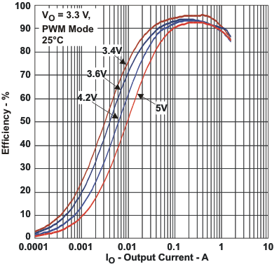 Figure 2. Efficiency DCDC1 vs Load Current/PWM Mode
 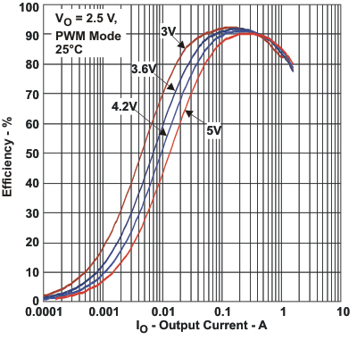 Figure 4. Efficiency DCDC2 vs Load Current/PWM Mode
 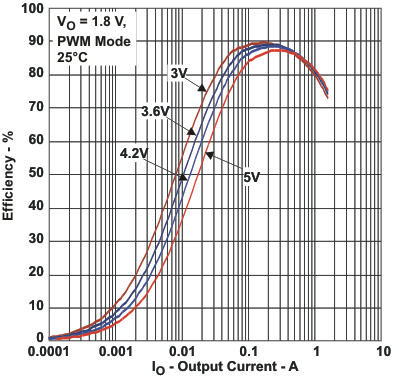 Figure 6. Efficiency DCDC2 vs Load Current/PWM Mode
 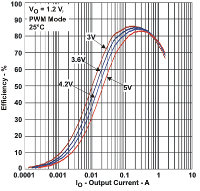 Figure 8. Efficiency DCDC3 vs Load Current/PWM Mode
 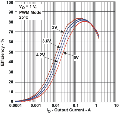 Figure 10. Efficiency DCDC3 vs Load Current/PWM Mode
 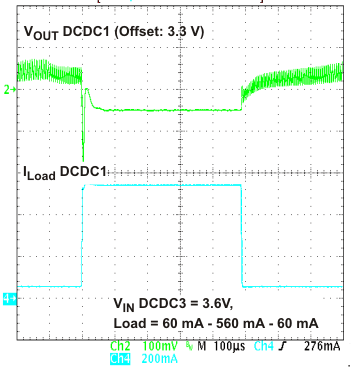 Figure 12. Load Transient Response Converter 1
 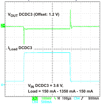 Figure 14. Load Transient Response Converter 3
 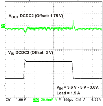 Figure 16. Line Transient Response Converter 2
 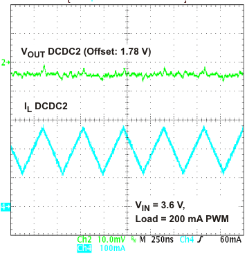 Figure 18. Output Voltage Ripple and Inductor Current Converter 2 – PWM Mode
 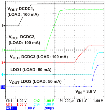 Figure 20. Startup DCDC1, DCDC2, AND DCDC3, LDO1, LDO2
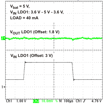
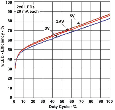 Figure 24. wLED Efficiency vs Duty Cycle
 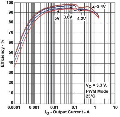 Figure 3. Efficiency DCDC1 vs Load Current/PFM Mode
 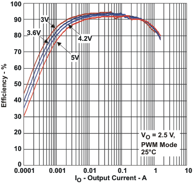 Figure 5. Efficiency DCDC2 vs Load Current/PFM Mode
 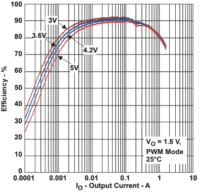 Figure 7. Efficiency DCDC2 vs Load Current/PFM Mode
 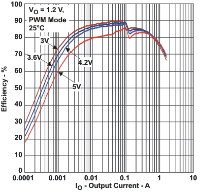 Figure 9. Efficiency DCDC3 vs Load Current/PFM Mode
 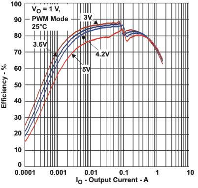 Figure 11. Efficiency DCDC3 vs Load Current/PFM Mode
 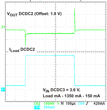 Figure 13. Load Transient Response Converter 2
 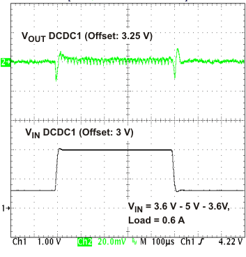 Figure 15. Line Transient Response Converter 1
 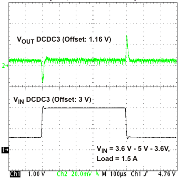 Figure 17. Line Transient Response Converter 3
 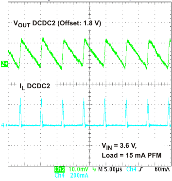 Figure 19. Output Voltage Ripple and Inductor Current Converter 2 – PFM Mode
 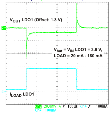 Figure 21. Load Transient Response LDO1
 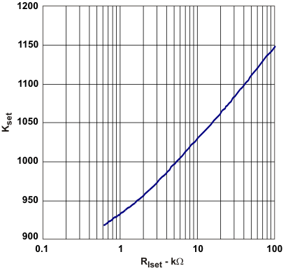 Figure 23. KSET vs RISET
 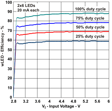 Figure 25. wLED Efficiency vs Vin