JAJSFO6G December 2015 – July 2024 TPS99000-Q1
PRODUCTION DATA
- 1
- 1 特長
- 2 アプリケーション
- 3 概要
- 4 Pin Configuration and Functions
-
5 Specifications
- 5.1 Absolute Maximum Ratings
- 5.2 ESD Ratings
- 5.3 Recommended Operating Conditions
- 5.4 Thermal Information
- 5.5 Electrical Characteristics—Transimpedance Amplifier Parameters
- 5.6 Electrical Characteristics—Digital to Analog Converters
- 5.7 Electrical Characteristics—Analog to Digital Converter
- 5.8 Electrical Characteristics—FET Gate Drivers
- 5.9 Electrical Characteristics—Photo Comparator
- 5.10 Electrical Characteristics—Voltage Regulators
- 5.11 Electrical Characteristics—Temperature and Voltage Monitors
- 5.12 Electrical Characteristics—Current Consumption
- 5.13 Power-Up Timing Requirements
- 5.14 Power-Down Timing Requirements
- 5.15 Timing Requirements—Sequencer Clock
- 5.16 Timing Requirements—Host and Diagnostic Port SPI Interface
- 5.17 Timing Requirements—ADC Interface
- 5.18 Switching Characteristics
-
6 Detailed Description
- 6.1 Overview
- 6.2 Functional Block Diagram
- 6.3
Feature Description
- 6.3.1
Illumination Control
- 6.3.1.1 Illumination System High Dynamic Range Dimming Overview
- 6.3.1.2 Illumination Control Loop
- 6.3.1.3 Continuous Mode Operation
- 6.3.1.4
Discontinuous Mode Operation
- 6.3.1.4.1 Discontinuous Mode Pulse Width Limit
- 6.3.1.4.2 COMPOUT_LOW Timer in Discontinuous Operation
- 6.3.1.4.3 Dimming Within Discontinuous Operation Range
- 6.3.1.4.4 Multiple Pulse Heights to Increase Bit Depth
- 6.3.1.4.5 TIA Gain Adjustment
- 6.3.1.4.6 Current Limit in Discontinuous Mode
- 6.3.1.4.7 CMODE Big Cap Mode in Discontinuous Operation
- 6.3.2 Over-Brightness Detection
- 6.3.3 Analog to Digital Converter
- 6.3.4 Power Sequencing and Monitoring
- 6.3.5 DMD Mirror Voltage Regulator
- 6.3.6 Low Dropout Regulators
- 6.3.7 System Monitoring Features
- 6.3.8 Communication Ports
- 6.3.1
Illumination Control
- 6.4 Device Functional Modes
- 6.5 Register Maps
- 7 Application and Implementation
- 8 Power Supply Recommendations
- 9 Layout
- 10Device and Documentation Support
- 11Revision History
- 12Mechanical, Packaging, and Orderable Information
9.1.4 High Power Current Loops
Due to the architecture of switched mode power supplies used to power the LED driver, there exist several current loops that can create interference. The best way to mitigate the effects of these loops is to minimize the area. Since the location of these loops is dependent on the LED drive architecture, the reader is referred to the data sheets of those parts for specific layout recommendation guidelines.
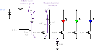
However, the TPS99000-Q1 does add an additional current loop which is specific to how it enables the LEDs in low brightness conditions. When operating the TPS99000-Q1 in discrete pulsed mode to achieve low light levels of LEDs, current flows through a shunt FET in the LED driver, creating a current loop that can inject noise into other circuits. The current loop is shown in Figure 9-1.
 Figure 9-1 Discontinuous Mode Current Loop
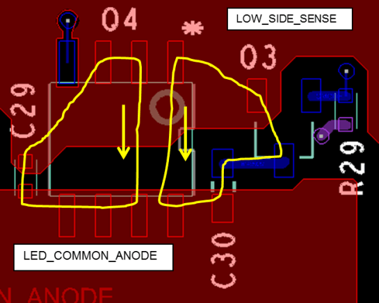
Here, the net LED_COMMON_ANODE is at the forward voltage of the LED when it is conducting current, and LOW_SIDE_SENSE is at near ground potential. When forming pulses in discrete pulsed mode, the S_EN1 FET redirects the current from the LED, causing it to turn off quickly. This has the added effect of discharging the 1μF capacitor, creating a brief, high current loop consisting of the S_EN1 FET, the CMODE FET, and the 1μF capacitor. There is also a secondary loop created by the S_EN1 FET and the 0.1μF capacitor. This set of components should be placed in a way to keep these loops small. One such possible placement is shown in Figure 9-2.
 Figure 9-2 High Power Layout