JAJSFV5C July   2018  – March 2022 UCC24624

PRODUCTION DATA  

  1. 特長
  2. アプリケーション
  3. 概要
  4. Revision History
  5. 概要 (続き)
  6. Pin Configuration and Functions
    1.     Pin Functions
  7. Specifications
    1. 7.1 Absolute Maximum Ratings
    2. 7.2 ESD Ratings
    3. 7.3 Recommended Operating Conditions
    4. 7.4 Thermal Information
    5. 7.5 Electrical Characteristics
    6. 7.6 Timing Requirements
    7. 7.7 Typical Characteristics
  8. Detailed Description
    1. 8.1 Overview
    2. 8.2 Functional Block Diagram
    3. 8.3 Feature Description
      1. 8.3.1 Power Management
      2. 8.3.2 Synchronous Rectifier Control
      3. 8.3.3 Turn-off Threshold Adjustment
      4. 8.3.4 Noise Immunity
        1. 8.3.4.1 On-Time Blanking
        2. 8.3.4.2 Off-Time Blanking
        3. 8.3.4.3 Two-Channel Interlock
        4. 8.3.4.4 SR Turn-on Re-arm
        5. 8.3.4.5 Adaptive Turn-on Delay
      5. 8.3.5 Gate Voltage Clamping
      6. 8.3.6 Standby Mode
    4. 8.4 Device Functional Modes
      1. 8.4.1 UVLO Mode
      2. 8.4.2 Standby Mode
      3. 8.4.3 Run Mode
  9. Application and Implementation
    1. 9.1 Application Information
    2. 9.2 Typical Application
      1. 9.2.1 Design Requirements
      2. 9.2.2 Detailed Design Procedure
        1. 9.2.2.1 MOSFET Selection
        2. 9.2.2.2 Snubber Design
      3. 9.2.3 Application Curves
  10. 10Power Supply Recommendations
  11. 11Layout
    1. 11.1 Layout Guidelines
    2. 11.2 Layout Example
  12. 12Device and Documentation Support
    1. 12.1 Device Support
      1. 12.1.1 Development Support
        1. 12.1.1.1 Custom Design With WEBENCH® Tools
    2. 12.2 Receiving Notification of Documentation Updates
    3. 12.3 Community Resources
    4. 12.4 Trademarks

Typical Characteristics

GUID-EF6846E8-9CEB-4BE2-9969-03D723AE5334-low.gif
Figure 7-1 UVLO Thresholds vs Temperature
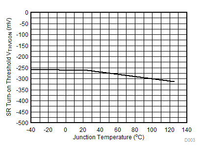
GUID-08431300-9F0F-4313-A24E-536D56E448B4-low.gifFigure 7-3 SR Turn-on Threshold Voltage vs Temperature
GUID-25791F6F-322C-4EDF-B514-CDE244E29435-low.gifFigure 7-5 Proportional Gate Drive Threshold vs Temperature
GUID-3F7903E6-27D8-4C04-8B2F-7C9214B22A3B-low.gif
ILOAD_REG = 10 mA
Figure 7-7 REG Dropout in Pass-through Mode vs Temperature
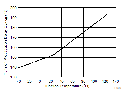
GUID-AEE49F56-276B-4AA3-A26C-D9015DEDC2D0-low.gifFigure 7-9 SR Turn-on Delay Time vs Temperature
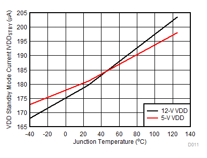
GUID-4A40AED5-854A-4537-A68F-AF61C132CC20-low.gifFigure 7-11 Standby Current vs Temperature
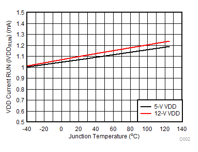
GUID-387C5065-3270-41BF-B797-2419212D6BAB-low.gif
CVG1 = CVG2 = 0 pFVVD1= VVD2 = 1 V
Figure 7-2 Bias Supply Current vs Temperature (No Switching)
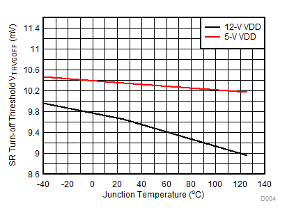
GUID-F8D903CB-3D4B-4B55-8B0B-98A8632B4650-low.gifFigure 7-4 SR Turn-off Threshold Voltages vs Temperature
GUID-C461F47B-D4DC-49D8-8D63-682DC94401C3-low.gifFigure 7-6 REG Pin Voltage vs Temperature at Different Loading Conditions
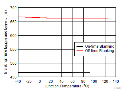
GUID-E7D7AE29-7680-4EDB-AA91-462CA8CC656E-low.gif
Figure 7-8 Blanking Time vs Temperature
GUID-38A7A27A-263D-46F9-B1AB-B0739A1458CB-low.gifFigure 7-10 SR Turn-off Propagation Delay vs Temperature
GUID-4BA7E0A7-F680-42A7-B9F4-124984ED98C4-low.gifFigure 7-12 VSS Pin Offset Current vs Temperature