JAJSFY4C August 2018 – October 2019 LMR36015-Q1
PRODUCTION DATA.
- 1 特長
- 2 アプリケーション
- 3 概要
- 4 改訂履歴
- 5 概要(続き)
- 6 Device Comparison Table
- 7 Pin Configuration and Functions
- 8 Specifications
- 9 Detailed Description
-
10Application and Implementation
- 10.1 Application Information
- 10.2
Typical Application
- 10.2.1
Design 1: Low Power 24-V, 1.5-A PFM Converter
- 10.2.1.1 Design Requirements
- 10.2.1.2
Detailed Design Procedure
- 10.2.1.2.1 Custom Design With WEBENCH Tools
- 10.2.1.2.2 Choosing the Switching Frequency
- 10.2.1.2.3 Setting the Output Voltage
- 10.2.1.2.4 Inductor Selection
- 10.2.1.2.5 Output Capacitor Selection
- 10.2.1.2.6 Input Capacitor Selection
- 10.2.1.2.7 CBOOT
- 10.2.1.2.8 VCC
- 10.2.1.2.9 CFF Selection
- 10.2.1.2.10 Maximum Ambient Temperature
- 10.2.2 Application Curves
- 10.2.3 Design 2: High Density 12-V, 1.5-A FPWM Converter
- 10.2.1
Design 1: Low Power 24-V, 1.5-A PFM Converter
- 10.3 What to Do and What Not to Do
- 11Power Supply Recommendations
- 12Layout
- 13デバイスおよびドキュメントのサポート
- 14メカニカル、パッケージ、および注文情報
9.1 Overview
The LMR36015-Q1 is a synchronous peak-current-mode buck regulator designed for a wide variety of automotive applications. The regulator automatically switches modes between PFM and PWM depending on load. At heavy loads, the device operates in PWM at a constant switching frequency. At light loads the mode changes to PFM, with diode emulation allowing DCM. This reduces the input supply current and keeps efficiency high. The device features internal loop compensation which reduces design time and requires fewer external components than externally compensated regulators.
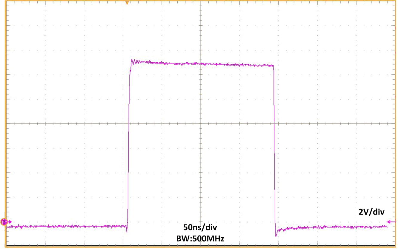
The LMR36015-Q1 is designed with a flip-chip or HotRod™ technology, greatly reducing the parasitic inductance of pins. In addition, the layout of the device allows for reduction in the radiated noise generated by the switching action through partial cancellation of the current generated magnetic field. As a result the switch-node waveform exhibits less overshoot and ringing.
 Figure 7. Switch Node Waveform