JAJSFZ6F May   2013  – August 2018 TS3DV642

PRODUCTION DATA.  

  1. 特長
  2. アプリケーション
  3. 概要
    1.     Device Images
      1.      概略回路図
  4. 改訂履歴
  5. Pin Configuration and Functions
    1.     Pin Functions
  6. Specifications
    1. 6.1 Absolute Maximum Ratings
    2. 6.2 ESD Ratings
    3. 6.3 Recommended Operating Conditions
    4. 6.4 Thermal Information
    5. 6.5 Electrical Characteristics
    6. 6.6 Dynamic Characteristics
    7. 6.7 Switching Characteristics
    8. 6.8 Typical Characteristics
  7. Parameter Measurement Information
  8. Detailed Description
    1. 8.1 Overview
    2. 8.2 Functional Block Diagram
    3. 8.3 Feature Description
    4. 8.4 Device Functional Modes
  9. Application and Implementation
    1. 9.1 Application Information
    2. 9.2 Typical Application
      1. 9.2.1 Display Port (DP) Application
        1. 9.2.1.1 Design Requirements
        2. 9.2.1.2 Detailed Design Procedure
        3. 9.2.1.3 Application Curves
      2. 9.2.2 Docking Application
        1. 9.2.2.1 Design Requirements
        2. 9.2.2.2 Detailed Design Procedure
        3. 9.2.2.3 Application Curves
      3. 9.2.3 HDMI Application
        1. 9.2.3.1 Design Requirements
        2. 9.2.3.2 Detailed Design Procedure
        3. 9.2.3.3 Application Curves
  10. 10Power Supply Recommendations
  11. 11Layout
    1. 11.1 Layout Guidelines
    2. 11.2 Layout Example
  12. 12デバイスおよびドキュメントのサポート
    1. 12.1 ドキュメントの更新通知を受け取る方法
    2. 12.2 コミュニティ・リソース
    3. 12.3 商標
    4. 12.4 静電気放電に関する注意事項
    5. 12.5 Glossary
  13. 13メカニカル、パッケージ、および注文情報

Typical Characteristics

TS3DV642 tc001_cds343.gif
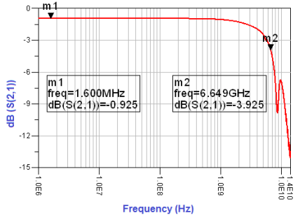
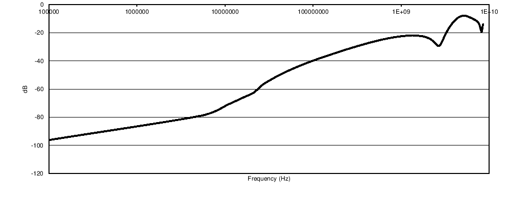
Figure 1. Differential S21 vs Frequency for Port A
TS3DV642 C001_SCDS343.png
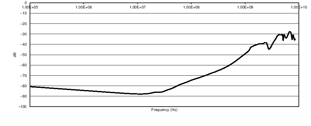
Figure 3. XTALK Port A
TS3DV642 C003_SCDS343.png
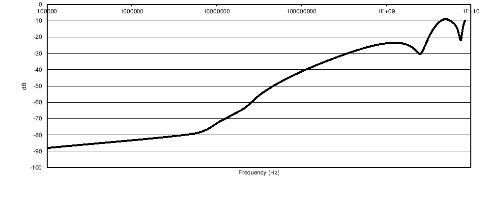
Figure 5. Off-State Isolation (OISO) for Port A
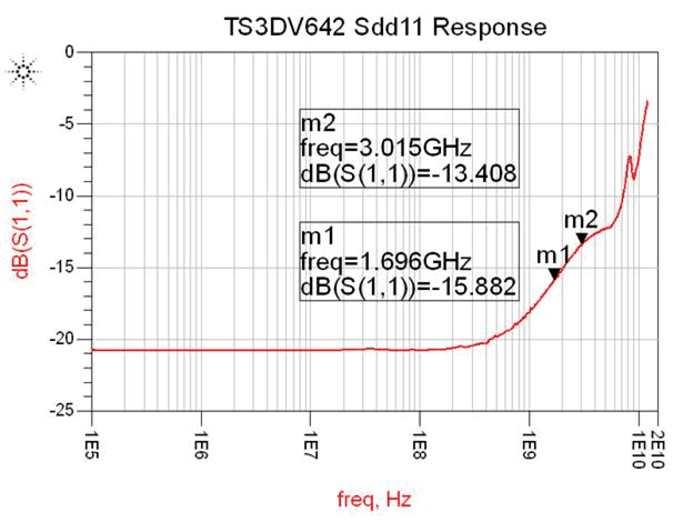
TS3DV642 SCDS343_returnloss.gifFigure 7. Return Loss (S11) Characteristics of TS3DV642
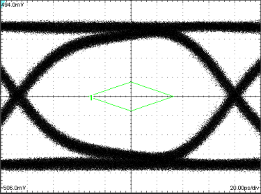
TS3DV642 tc2_scds343.gifFigure 9. Eye Pattern: 6.0 Gbps, No Device Through Path (Only One Channel Measured at a Time)
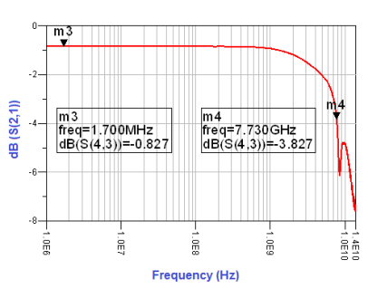
TS3DV642 tc002_cds343.gif
Figure 2. Differential S21 vs Frequency for Port B
TS3DV642 C002_SCDS343.png
Figure 4. XTALK Port B
TS3DV642 C004_SCDS343.png
Figure 6. Off-State Isolation (OISO) for Port B
TS3DV642 tc1_scds343.gif
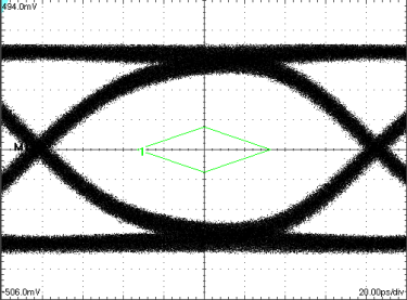
Figure 8. Eye Pattern: 6.0 Gbps Port A, D1+ to D1+A, D1- to D1-A (Only One Channel Measured at a Time)
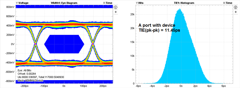
TS3DV642 A_wDevice_cds343.pngFigure 10. Eye Pattern and Time Interval Error Histogram: 3.4 Gbps Port A, With Device
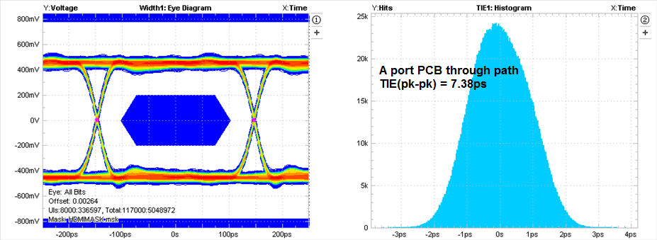
TS3DV642 A_woDevice_cds343.pngFigure 11. Eye Pattern and Time Interval Error Histogram: 3.4 Gbps, No Device Through Path
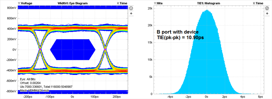
TS3DV642 B_wDevice_cds343.pngFigure 12. Eye Pattern and Time Interval Error Histogram: 3.4 Gbps Port B, With Device
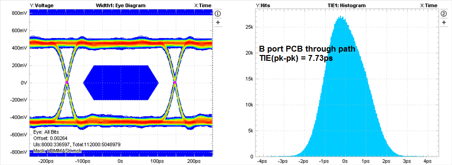
TS3DV642 B_woDevice_cds343.pngFigure 13. Eye Pattern and Time Interval Error Histogram: 3.4 Gbps Port B, No Device