JAJSG97A September   2018  – March 2019 LMG3410R050 , LMG3411R050

ADVANCE INFORMATION for pre-production products; subject to change without notice.  

  1. 特長
  2. アプリケーション
  3. 概要
    1.     Device Images
      1.      ブロック概略図
      2.      100V/nsを超えるスイッチング性能
  4. 改訂履歴
  5. Pin Configuration and Functions
    1.     Pin Functions
  6. Specifications
    1. 6.1 Absolute Maximum Ratings
    2. 6.2 ESD Ratings
    3. 6.3 Recommended Operating Conditions
    4. 6.4 Thermal Information
    5. 6.5 Electrical Characteristics
    6. 6.6 Switching Characteristics
  7. Parameter Measurement Information
    1. 7.1 Switching Parameters
      1. 7.1.1 Turn-on Delays
      2. 7.1.2 Turn-off Delays
      3. 7.1.3 Drain Slew Rate
  8. Detailed Description
    1. 8.1 Overview
    2. 8.2 Functional Block Diagram
    3. 8.3 Feature Description
      1. 8.3.1 Direct-Drive GaN Architecture
      2. 8.3.2 Internal Buck-Boost DC-DC Converter
      3. 8.3.3 Internal Auxiliary LDO
      4. 8.3.4 Fault Detection
        1. 8.3.4.1 Over-current Protection
        2. 8.3.4.2 Over-Temperature Protection and UVLO
      5. 8.3.5 Drive Strength Adjustment
    4. 8.4 Device Functional Modes
      1. 8.4.1 Low-Power Mode
  9. Application and Implementation
    1. 9.1 Application Information
    2. 9.2 Typical Application
      1. 9.2.1 Design Requirements
      2. 9.2.2 Detailed Design Procedure
        1. 9.2.2.1 Slew Rate Selection
          1. 9.2.2.1.1 Startup and Slew Rate with Bootstrap High-Side Supply
        2. 9.2.2.2 Signal Level-Shifting
        3. 9.2.2.3 Buck-Boost Converter Design
      3. 9.2.3 Application Curves
    3. 9.3 Paralleling GaN Devices
    4. 9.4 Do's and Don'ts
  10. 10Power Supply Recommendations
    1. 10.1 Using an Isolated Power Supply
    2. 10.2 Using a Bootstrap Diode
      1. 10.2.1 Diode Selection
      2. 10.2.2 Managing the Bootstrap Voltage
      3. 10.2.3 Reliable Bootstrap Start-up
  11. 11Layout
    1. 11.1 Layout Guidelines
      1. 11.1.1 Power Loop Inductance
      2. 11.1.2 Signal Ground Connection
      3. 11.1.3 Bypass Capacitors
      4. 11.1.4 Switch-Node Capacitance
      5. 11.1.5 Signal Integrity
      6. 11.1.6 High-Voltage Spacing
      7. 11.1.7 Thermal Recommendations
    2. 11.2 Layout Example
  12. 12デバイスおよびドキュメントのサポート
    1. 12.1 デバイス・サポート
      1. 12.1.1 デベロッパー・ネットワークの製品に関する免責事項
    2. 12.2 ドキュメントのサポート
      1. 12.2.1 関連資料
    3. 12.3 ドキュメントの更新通知を受け取る方法
    4. 12.4 コミュニティ・リソース
    5. 12.5 商標
    6. 12.6 静電気放電に関する注意事項
    7. 12.7 Glossary
  13. 13メカニカル、パッケージ、および注文情報

Pin Configuration and Functions

RWH (QFN) PACKAGE
32 PINS
(Top View)
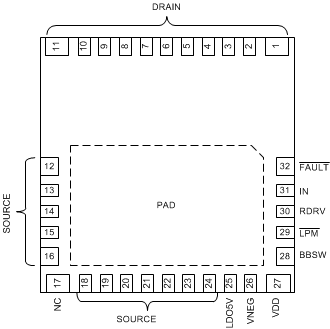
LMG3410R050 LMG3411R050 pin_diagram_snosd10.gif

Pin Functions

PIN I/O(1) DESCRIPTION
NAME NO.
BBSW 28 P Internal buck-boost converter switch pin. Connect an inductor from this point to source
DRAIN 1-11 P Power transistor drain
FAULT 32 O Fault output, push-pull, active low
IN 31 I CMOS-compatible non-inverting gate drive input
LDO5V 25 P 5-V LDO output for external digital isolator.
LPM 29 I Enables low-power-mode by connecting the pin to source
SOURCE 12-16, 18-24 P Power transistor source, die-attach pad, thermal sink, signal ground reference
RDRV 30 I Drive strength selection pin. Connect a resistor from this pin to ground to set the turn-on drive strength to control slew rate,
VDD 27 P 12-V power input, relative to source. Supplies 5-V rail and gate drive supply.
VNEG 26 P Negative supply output, bypass to source with 2.2-µF capacitor
NC 17 Not connected, connect to source or leave floating.
PAD P Thermal Pad, tie to source with multiple vias.
I = Input, O = Output, P = Power