JAJSGA2F September 2018 – June 2021 TPS2663
PRODUCTION DATA
- 1 特長
- 2 アプリケーション
- 3 概要
- 4 Revision History
- 5 Device Comparison Table
- 6 Pin Configuration and Functions
- 7 Specifications
- 8 Parameter Measurement Information
-
9 Detailed Description
- 9.1 Overview
- 9.2 Functional Block Diagram
- 9.3
Feature Description
- 9.3.1 Hot Plug-In and In-Rush Current Control
- 9.3.2 PGOOD and PGTH
- 9.3.3 Undervoltage Lockout (UVLO)
- 9.3.4 Overvoltage Protection (OVP)
- 9.3.5 Input Reverse Polarity Protection (B_GATE, DRV)
- 9.3.6 Reverse Current Protection
- 9.3.7 Overload and Short Circuit Protection
- 9.3.8 Output Power Limiting, PLIM (TPS26632, TPS26633, TPS26635 and TPS26636 Only)
- 9.3.9 Current Monitoring Output (IMON)
- 9.3.10 FAULT Response ( FLT)
- 9.3.11 IN_SYS, IN, OUT and GND Pins
- 9.3.12 Thermal Shutdown
- 9.3.13 Low Current Shutdown Control (SHDN)
- 9.4 Device Functional Modes
-
10Application and Implementation
- 10.1 Application Information
- 10.2
Typical Application: Power Path Protection in a PLC System
- 10.2.1 Design Requirements
- 10.2.2 Detailed Design Procedure
- 10.2.3 Application Curves
- 10.3 System Examples
- 10.4 Do's and Don'ts
- 11Power Supply Recommendations
- 12Layout
- 13Device and Documentation Support
- 14Mechanical, Packaging, and Orderable Information
9.3.13 Low Current Shutdown Control (SHDN)
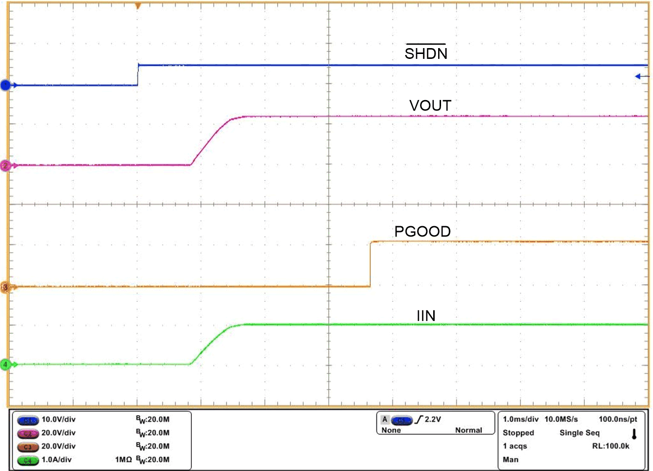
The internal, external FET and hence the load current can be switched off by pulling the SHDN pin below 0.8-V threshold with a micro-controller GPIO pin or can be controlled remotely with an opto-isolator device. The device quiescent current reduces to 21 μA (typical) in shutdown state. To assert SHDN low, the pull down must have sinking capability of at least 10 µA. To enable the device, SHDN must be pulled up to at least 2 V. Once the device is enabled, the internal FET turns on with dVdT mode. Figure 9-20 and Figure 9-13 illustrate the performance of SHDN control.

| VIN = 24 V | C(dVdT) = 22 nF | RLOAD = 24 Ω |

| VIN = 24 V | C(dVdT) = 22 nF | RLOAD = 24 Ω |