JAJSGA9C September   2018  – September 2019 ISO1500

PRODUCTION DATA.  

  1. 特長
  2. アプリケーション
  3. 概要
    1.     概略回路図
  4. 改訂履歴
  5. 概要 (続き)
  6. Pin Configuration and Functions
    1.     Pin Functions
  7. Specifications
    1. 7.1  Absolute Maximum Ratings
    2. 7.2  ESD Ratings
    3. 7.3  Recommended Operating Conditions
    4. 7.4  Thermal Information
    5. 7.5  Power Ratings
    6. 7.6  Insulation Specifications
    7. 7.7  Safety-Related Certifications
    8. 7.8  Safety Limiting Values
    9. 7.9  Electrical Characteristics: Driver
    10. 7.10 Electrical Characteristics: Receiver
    11. 7.11 Supply Current Characteristics: Side 1(ICC1)
    12. 7.12 Supply Current Characteristics: Side 2(ICC2)
    13. 7.13 Switching Characteristics: Driver
    14. 7.14 Switching Characteristics: Receiver
    15. 7.15 Insulation Characteristics Curves
    16. 7.16 Typical Characteristics
  8. Parameter Measurement Information
  9. Detailed Description
    1. 9.1 Overview
    2. 9.2 Functional Block Diagram
    3. 9.3 Feature Description
      1. 9.3.1 Electromagnetic Compatibility (EMC) Considerations
      2. 9.3.2 Failsafe Receiver
      3. 9.3.3 Thermal Shutdown
      4. 9.3.4 Glitch-Free Power Up and Power Down
    4. 9.4 Device Functional Modes
      1. 9.4.1 Device I/O Schematics
  10. 10Application and Implementation
    1. 10.1 Application Information
    2. 10.2 Typical Application
      1. 10.2.1 Design Requirements
      2. 10.2.2 Detailed Design Procedure
        1. 10.2.2.1 Data Rate and Bus Length
        2. 10.2.2.2 Stub Length
        3. 10.2.2.3 Bus Loading
  11. 11Power Supply Recommendations
  12. 12Layout
    1. 12.1 Layout Guidelines
      1. 12.1.1 PCB Material
    2. 12.2 Layout Example
  13. 13デバイスおよびドキュメントのサポート
    1. 13.1 ドキュメントのサポート
      1. 13.1.1 関連資料
    2. 13.2 ドキュメントの更新通知を受け取る方法
    3. 13.3 コミュニティ・リソース
    4. 13.4 商標
    5. 13.5 静電気放電に関する注意事項
    6. 13.6 Glossary
  14. 14メカニカル、パッケージ、および注文情報

Typical Characteristics

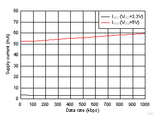
ISO1500 D015_SLLSF21.gif
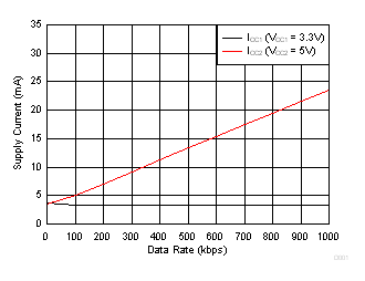
TA = 25°C DE = VCC1 RE = GND1
Figure 3. Supply Current Vs Data Rate- No Load
ISO1500 D003_SLLSF21.gif
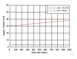
TA = 25°C DE = VCC1 RE = GND1
Driver load = 120 ohm || 50 pF Load on R = 15 pF
Figure 5. Supply Current Vs Data Rate - with 120 Ω || 50 pf Load
ISO1500 D004_SLLSF21.gif
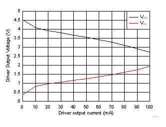
DE = VCC1 D = GND1 VCC1 = 3.3 V
VCC2 = 5 V TA = 25°C
Figure 7. Driver Output Voltage Vs Driver Output Current
ISO1500 D007_SLLSF21.gif
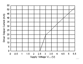
TA = 25°C RL = 54 ohm DE = D = VCC1
Figure 9. Driver Output Current Vs Supply Voltage (VCC2)
ISO1500 D009_SLLSF21.gif
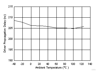
VCC1 = 3.3 V VCC2 = 5 V
Figure 11. Driver Propagation Delay vs Temperature
ISO1500 D013_SLLSF21.gif
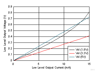
TA = 25°C
Figure 13. Receiver Buffer Low Level Output Voltage Vs Low Level Output Current
ISO1500 iso1500-driver-propagation-delay.png
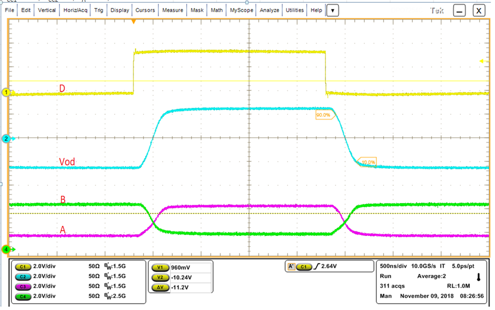
VCC1 = 3.3 V VCC2 = 5 V DE = VCC1
TA = 25°C
Figure 15. Driver Propagation delay
ISO1500 iso14xx-vcc1-power-up-power-down-glitch-free-behavior.png
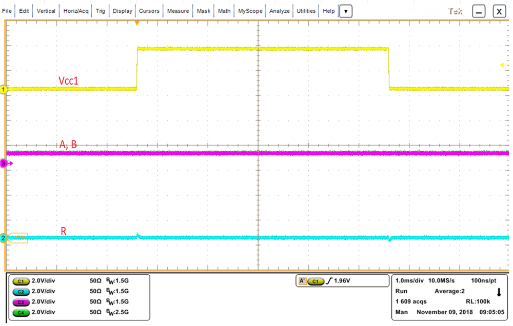
Figure 17. VCC1 Power Up / Power down- Glitch Free Behavior
ISO1500 D016_SLLSF21.gif
TA = 25°C DE = VCC1 RE = GND1
Driver load = 54 ohm || 50 pF Load on R = 15 pF
Figure 4. Supply Current Vs Data Rate- with 54 Ω || 50 pf Load
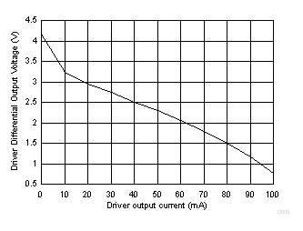
ISO1500 D005_SLLSF21.gif
DE = VCC1 D = GND1 VCC1 = 3.3 V
VCC2 = 5 V TA = 25°C
Figure 6. Driver Differential Output Voltage Vs Driver Output Current
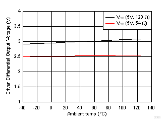
ISO1500 D006_SLLSF21.gif
Figure 8. Driver Differential Output Voltage Vs Temperature
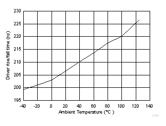
ISO1500 D008_SLLSF21.gif
VCC1 = 3.3 V VCC2 = 5 V
Figure 10. Driver rise/fall time vs Temperature
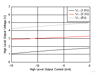
ISO1500 D010_SLLSF21.gif
TA = 25°C
Figure 12. Receiver Buffer High Level Output Voltage Vs High Level Output Current
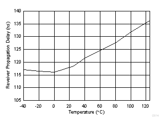
ISO1500 D014_SLLSF21.gif
VCC1 = 3.3 V VCC2 = 5 V
Figure 14. Receiver Propagation Delay Vs Temperature
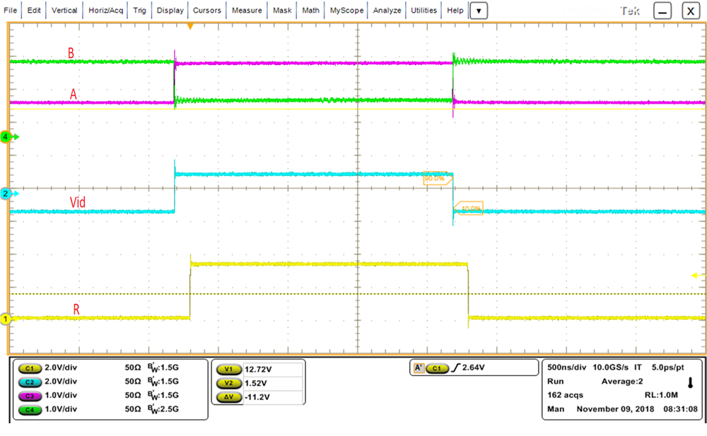
ISO1500 iso1500-receiver-propagation-delay.png
VCC1 = 3.3 V VCC2 = 5 V TA = 25°C,
DE = GND1 RE = GND1
Figure 16. Receiver Propagation Delay
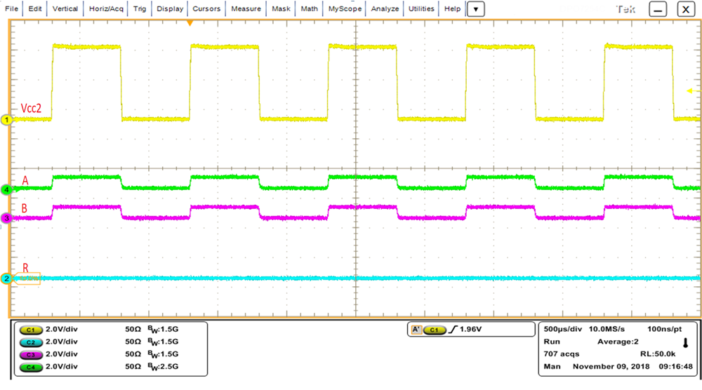
ISO1500 iso14xx-vcc2-power-up-power-down-glitch-free-behavior.png
Figure 18. VCC2 Power Up / Power down- Glitch Free Behavior