JAJSGP0D December   2017  – July 2021 TLV767

PRODUCTION DATA  

  1. 特長
  2. アプリケーション
  3. 概要
  4. Revision History
  5. Pin Configuration and Functions
  6. Specifications
    1. 6.1 Absolute Maximum Ratings
    2. 6.2 ESD Ratings
    3. 6.3 Recommended Operating Conditions
    4. 6.4 Thermal Information
    5. 6.5 Electrical Characteristics
  7. Typical Characteristics
  8. Detailed Description
    1. 8.1 Overview
    2. 8.2 Functional Block Diagrams
    3. 8.3 Feature Description
      1. 8.3.1 Output Enable
      2. 8.3.2 Dropout Voltage
      3. 8.3.3 Foldback Current Limit
      4. 8.3.4 Undervoltage Lockout (UVLO)
      5. 8.3.5 Output Pulldown
      6. 8.3.6 Thermal Shutdown
    4. 8.4 Device Functional Modes
      1. 8.4.1 Device Functional Mode Comparison
      2. 8.4.2 Normal Operation
      3. 8.4.3 Dropout Operation
      4. 8.4.4 Disabled
  9. Application and Implementation
    1. 9.1 Application Information
      1. 9.1.1 Adjustable Device Feedback Resistors
      2. 9.1.2 Recommended Capacitor Types
      3. 9.1.3 Input and Output Capacitor Requirements
      4. 9.1.4 Reverse Current
      5. 9.1.5 Feed-Forward Capacitor (CFF)
      6. 9.1.6 Power Dissipation (PD)
      7. 9.1.7 Estimating Junction Temperature
    2. 9.2 Typical Application
      1. 9.2.1 Design Requirements
      2. 9.2.2 Detailed Design Procedure
        1. 9.2.2.1 Transient Response
        2. 9.2.2.2 Choose Feedback Resistors
      3. 9.2.3 Application Curves
  10. 10Power Supply Recommendations
  11. 11Layout
    1. 11.1 Layout Guidelines
    2. 11.2 Layout Examples
  12. 12Device and Documentation Support
    1. 12.1 Device Support
      1. 12.1.1 Device Nomenclature
    2. 12.2 Documentation Support
      1. 12.2.1 Related Documentation
    3. 12.3 Receiving Notification of Documentation Updates
    4. 12.4 サポート・リソース
    5. 12.5 Trademarks
    6. 12.6 Electrostatic Discharge Caution
    7. 12.7 Glossary

Typical Characteristics

at operating temperature TJ = 25°C, VIN = VOUT(NOM) + 1.5 V or 2.5 V (whichever is greater), IOUT = 10 mA, VEN = 2.0 V, CIN = 1.0 µF, and COUT = 1.0 µF (unless otherwise noted)

GUID-A9BE9C88-DFDF-40AB-B0B1-FD2C39F7B018-low.gif
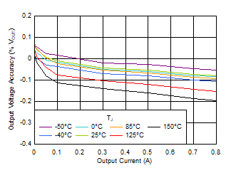
VIN = 3.0 V
Figure 7-1 VOUT Accuracy vs IOUT
GUID-DD8ECAFF-C847-4976-8E3F-0C436DC74E2B-low.gif
IOUT = 10 mA
Figure 7-3 VOUT Accuracy vs VIN
GUID-1FAC2116-0629-4DDF-949D-72893B2197B1-low.gif
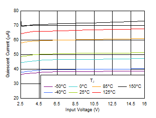
IOUT = 0 mA, adjustable-voltage version devices
Figure 7-5 IQ vs VIN
GUID-6D8AF07B-0503-4BB9-9419-E903EBB07F4B-low.gif
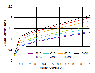
VIN = 3.0 V
Figure 7-7 IGND vs IOUT
GUID-D93F026D-88C3-4CC9-A4BD-A59E1CDDEEB5-low.gif
IOUT = 0 mA
Figure 7-9 IQ Increase Below Minimum VIN
GUID-38E8FE24-1D8B-4DDA-AB43-0E5F1BC2FDDB-low.gif
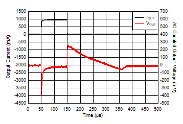
VIN = 5 V, VOUT = 3.3 V, CFF = 10 pF, ramp rate = 0.5 A/µs
Figure 7-11 IOUT Transient From 1 mA to 1 A
GUID-555686DF-121C-4FEC-B828-D4012C888521-low.gif
VOUT = 3.3 V, IOUT = 1 A, VIN ramp rate = 0.6 V/µs
Figure 7-13 VIN Transient in Dropout From 4 V to 13 V
GUID-CD58D1F7-EC34-4961-8F0E-D16B2F096440-low.gif
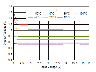
IOUT = 1.0 A
Figure 7-15 VDO vs VIN
GUID-EBCD7610-C682-4191-B1E4-4ECA12B583BF-low.gif
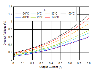
VIN = 3.0 V
Figure 7-17 VDO vs IOUT
GUID-0B35547B-1039-430E-8469-8E3B785A3BAC-low.gif
VIN = 3.0 V
Figure 7-19 Foldback Current Limit vs Temperature
GUID-27DFA498-4B2C-40A7-99B7-A1A738E7786B-low.gif
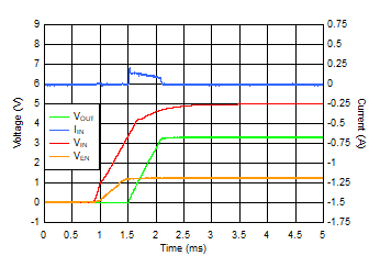
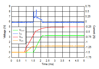
VOUT = 3.3 V
Figure 7-21 Startup With Separate VEN and VIN
GUID-EC4AF611-0818-4734-A21D-2B7C8921BB99-low.gif
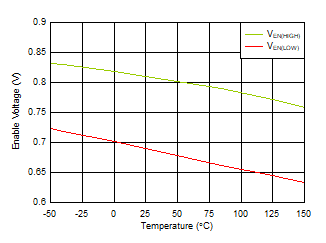
VIN = 2.5 V
Figure 7-23 VEN Thresholds vs Temperature
GUID-8C80948B-FA01-4625-87C6-21082290EE9C-low.gif
 
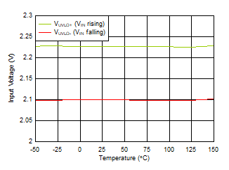
Figure 7-25 UVLO Thresholds vs Temperature
GUID-C11F64B7-9AB7-4175-BAFD-9E4726A105DF-low.gif
VOUT = 1.8 V, IOUT = 0.55 A, CFF = 1 nF
Figure 7-27 PSRR vs VIN
GUID-0B1A6D93-1C1D-447E-A380-AFB0FE101D32-low.gif
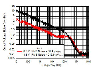
CFF = 0 nF, IOUT = 0.1 A, RMS noise BW = 10 Hz to 100 kHz
Figure 7-29 Output Noise (Vn) vs VOUT
GUID-D4C4743F-42D4-40CA-8385-FF2971562841-low.gif
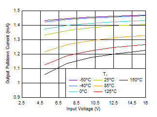
VOUT = 2.5 V
Figure 7-31 IPULLDOWN vs VIN
GUID-D306DDA5-9A18-4C93-8F93-E717C4E9E1CA-low.gif
VOUT = 3.3 V, IOUT = 33 µA
Figure 7-33 Startup Inrush Current With COUT = 22 µF
GUID-B573F720-919E-44E4-8F5F-B405F962DCF5-low.gif
VIN = 2.5 V
Figure 7-2 VOUT Accuracy vs IOUT
GUID-4A4546F4-9F6B-4A40-A578-46BD70403893-low.gifFigure 7-4 ISHUTDOWN vs VIN
GUID-09FC5A0D-D517-4B6E-8DBA-41A40CFC366E-low.gif
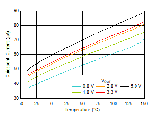
IOUT = 0 mA, fixed-voltage version devices
Figure 7-6 IQ vs Temperature
GUID-76D96B98-B635-4D0D-9FB3-78ECD4B7D21A-low.gif
VIN = 2.5 V
Figure 7-8 IGND vs IOUT
GUID-4E0C95F3-D90A-4662-8034-EC165CDCAE23-low.gif
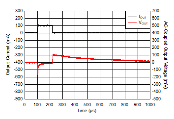
VIN = 5 V, VOUT = 3.3 V, CFF = 10 pF, ramp rate = 0.4 A/µs
Figure 7-10 IOUT Transient From 0 mA to 100 mA
GUID-00D20450-D1D2-4E20-8D90-992090FC667E-low.gif
VIN = 5 V, VOUT = 3.3 V, ramp rate = 0.8 A/µs
Figure 7-12 IOUT Transient From 250 mA to 850 mA
GUID-B953D543-AE30-4766-9C93-D23A636A5915-low.gif
VOUT = 3.3 V, IOUT = 33 µA, VIN ramp rate = 1.6 V/µs
Figure 7-14 VIN Transient From 5 V to 16 V
GUID-2A09DD0F-B666-473D-94A6-565533ABF5CE-low.gif
IOUT = 0.8 A
Figure 7-16 VDO vs VIN
GUID-9B0C39AD-D8B2-4141-A099-88337700B550-low.gif
VIN = 2.5 V
Figure 7-18 VDO vs IOUT
GUID-D1213678-85B7-4F19-A35E-1D0D7F71EBFE-low.gif
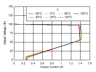
VIN = 2.5 V
Figure 7-20 Foldback Current Limit vs Temperature
GUID-D7F0EAF6-A677-45EE-8F65-E9E29F6A85CD-low.gif
Enable pulled up internally, VOUT = 0.8 V
Figure 7-22 Startup With VEN Floating
GUID-484F0A3D-CC68-4FDE-A6B4-8CF750C30B5E-low.gif
VIN = 16 V
Figure 7-24 VEN Thresholds vs Temperature
GUID-F2A34B7E-03DD-423B-8318-65B3B6517824-low.gif
VOUT = 1.8 V, VIN = 3.3 V, CFF = 1 nF
Figure 7-26 PSRR vs IOUT
GUID-A46C164B-C446-4285-8C79-F43A0C26C29B-low.gif
VOUT = 3.3 V, VIN = 4.8 V, IOUT = 0.33 A
Figure 7-28 PSRR vs CFF
GUID-913D9C67-C692-4F9F-9EF8-2A52AED2FD1B-low.gif
VEN = 0 V
Figure 7-30 IEN vs VIN
GUID-3ABD98A9-D5E3-41CA-9723-24F1DF9AAC59-low.gif
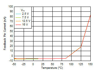
VFB = 1.0 V
Figure 7-32 IFB vs Temperature
GUID-989B824E-FD01-4EBF-9D4A-67375547BDAD-low.gif
VOUT = 3.3 V, IOUT = 33 µA
Figure 7-34 Startup Inrush Current With COUT = 47 µF