JAJSGP0D
December 2017 – July 2021
TLV767
PRODUCTION DATA
1
特長
2
アプリケーション
3
概要
4
Revision History
5
Pin Configuration and Functions
6
Specifications
6.1
Absolute Maximum Ratings
6.2
ESD Ratings
6.3
Recommended Operating Conditions
6.4
Thermal Information
6.5
Electrical Characteristics
7
Typical Characteristics
8
Detailed Description
8.1
Overview
8.2
Functional Block Diagrams
8.3
Feature Description
8.3.1
Output Enable
8.3.2
Dropout Voltage
8.3.3
Foldback Current Limit
8.3.4
Undervoltage Lockout (UVLO)
8.3.5
Output Pulldown
8.3.6
Thermal Shutdown
8.4
Device Functional Modes
8.4.1
Device Functional Mode Comparison
8.4.2
Normal Operation
8.4.3
Dropout Operation
8.4.4
Disabled
9
Application and Implementation
9.1
Application Information
9.1.1
Adjustable Device Feedback Resistors
9.1.2
Recommended Capacitor Types
9.1.3
Input and Output Capacitor Requirements
9.1.4
Reverse Current
9.1.5
Feed-Forward Capacitor (CFF)
9.1.6
Power Dissipation (PD)
9.1.7
Estimating Junction Temperature
9.2
Typical Application
9.2.1
Design Requirements
9.2.2
Detailed Design Procedure
9.2.2.1
Transient Response
9.2.2.2
Choose Feedback Resistors
9.2.3
Application Curves
10
Power Supply Recommendations
11
Layout
11.1
Layout Guidelines
11.2
Layout Examples
12
Device and Documentation Support
12.1
Device Support
12.1.1
Device Nomenclature
12.2
Documentation Support
12.2.1
Related Documentation
12.3
Receiving Notification of Documentation Updates
12.4
サポート・リソース
12.5
Trademarks
12.6
Electrostatic Discharge Caution
12.7
Glossary
9.2.3
Application Curves
V
IN
= 5 V, V
OUT
= 3.3 V, C
OUT
= 1 µF, C
FF
= 10 pF
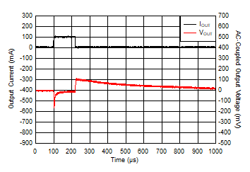
Figure 9-3
Load Transient Response, I
OUT
0 mA to 100 mA
V
IN
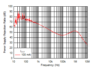
= 5 V, V
OUT
= 3.3 V, C
OUT
= 1 µF, C
FF
= 0 pF
Figure 9-4
PSRR Performance