JAJSGU3H March 2012 – March 2019 SN65HVD72 , SN65HVD75 , SN65HVD78
UNLESS OTHERWISE NOTED, this document contains PRODUCTION DATA.
- 1 特長
- 2 アプリケーション
- 3 概要
- 4 改訂履歴
- 5 Device Comparison Table
- 6 Pin Configuration and Functions
-
7 Specifications
- 7.1 Absolute Maximum Ratings
- 7.2 ESD Ratings
- 7.3 Recommended Operating Conditions
- 7.4 Thermal Information
- 7.5 Electrical Characteristics
- 7.6 Power Dissipation
- 7.7 Switching Characteristics: 250 kbps Device (SN65HVD72) Bit Time ≥ 4 µs
- 7.8 Switching Characteristics: 20 Mbps Device (SN65HVD75) Bit Time ≥50 ns
- 7.9 Switching Characteristics: 50 Mbps Device (SN65HVD78) Bit Time ≥20 ns
- 7.10 Typical Characteristics
- 8 Parameter Measurement Information
- 9 Detailed Description
- 10Application and Implementation
- 11Power Supply Recommendations
- 12Layout
- 13デバイスおよびドキュメントのサポート
- 14メカニカル、パッケージ、および注文情報
8 Parameter Measurement Information
Input generator rate is 100 kbps, 50% duty cycle, rise or fall time is less than 6 ns, output impedance is 50 Ω.
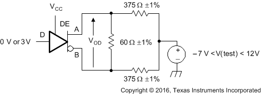
 Figure 10. Measurement of Driver Differential Output Voltage With Common-Mode Load
  Figure 11. Measurement of Driver Differential and Common-Mode Output With RS-485 Load
  Figure 12. Measurement of Driver Differential Output Rise and Fall Times and Propagation Delays
D at 3 V to test non-inverting output, D at 0 V to test inverting output.
Figure 13. Measurement of Driver Enable and Disable Times With Active High Output and Pulldown Load 
D at 0 V to test non-inverting output, D at 3 V to test inverting output.
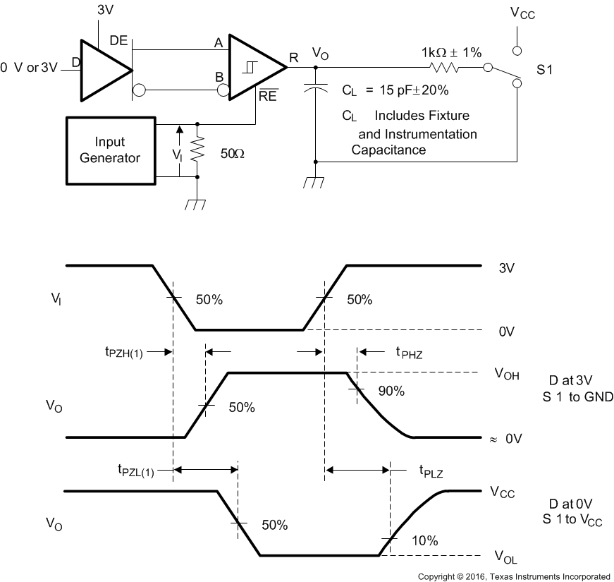
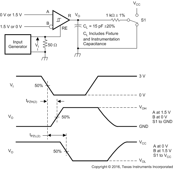
Figure 14. Measurement of Driver Enable and Disable Times With Active Low Output and Pullup Load  Figure 15. Measurement of Receiver Output Rise and Fall Times and Propagation Delays
  Figure 16. Measurement of Receiver Enable and Disable Times With Driver Enabled
  Figure 17. Measurement of Receiver Enable Times With Driver Disabled