JAJSGX1G September   2006  – Jaunuary 2020 LM5069

PRODUCTION DATA.  

  1. 特長
  2. アプリケーション
  3. 概要
    1.     Device Images
      1.      代表的なアプリケーションの図
  4. 改訂履歴
    1.     Device Comparison
  5. Pin Configuration and Functions
    1.     Pin Functions
  6. Specifications
    1. 6.1 Absolute Maximum Ratings
    2. 6.2 ESD Ratings
    3. 6.3 Recommended Operating Conditions
    4. 6.4 Thermal Information
    5. 6.5 Electrical Characteristics
    6. 6.6 Typical Characteristics
  7. Detailed Description
    1. 7.1 Overview
    2. 7.2 Functional Block Diagram
    3. 7.3 Feature Description
      1. 7.3.1 Current Limit
      2. 7.3.2 Circuit Breaker
      3. 7.3.3 Power Limit
      4. 7.3.4 Undervoltage Lockout (UVLO)
      5. 7.3.5 Overvoltage Lockout (OVLO)
      6. 7.3.6 Power Good Pin
    4. 7.4 Device Functional Modes
      1. 7.4.1 Power Up Sequence
      2. 7.4.2 Gate Control
      3. 7.4.3 Fault Timer and Restart
      4. 7.4.4 Shutdown Control
  8. Application and Implementation
    1. 8.1 Application Information
    2. 8.2 Typical Application
      1. 8.2.1 48-V, 10-A Hot Swap Design
        1. 8.2.1.1 Design Requirements
        2. 8.2.1.2 Detailed Design Procedure
          1. 8.2.1.2.1 Select RSNS and CL setting
          2. 8.2.1.2.2 Selecting the Hot Swap FET(s)
          3. 8.2.1.2.3 Select Power Limit
          4. 8.2.1.2.4 Set Fault Timer
          5. 8.2.1.2.5 Check MOSFET SOA
          6. 8.2.1.2.6 Set Undervoltage and Overvoltage Threshold
            1. 8.2.1.2.6.1 Option A
            2. 8.2.1.2.6.2 Option B
            3. 8.2.1.2.6.3 Option C
            4. 8.2.1.2.6.4 Option D
          7. 8.2.1.2.7 Input and Output Protection
          8. 8.2.1.2.8 Final Schematic and Component Values
        3. 8.2.1.3 Application Curves
  9. Power Supply Recommendations
  10. 10Layout
    1. 10.1 Layout Guidelines
      1. 10.1.1 PC Board Guidelines
      2. 10.1.2 System Considerations
    2. 10.2 Layout Example
  11. 11デバイスおよびドキュメントのサポート
    1. 11.1 デバイス・サポート
      1. 11.1.1 開発サポート
    2. 11.2 ドキュメントのサポート
      1. 11.2.1 関連資料
    3. 11.3 ドキュメントの更新通知を受け取る方法
    4. 11.4 コミュニティ・リソース
    5. 11.5 商標
    6. 11.6 静電気放電に関する注意事項
    7. 11.7 Glossary
  12. 12メカニカル、パッケージ、および注文情報

Check MOSFET SOA

Once the power limit and fault timer are chosen, it’s critical to check that the FET stays within its SOA during all test conditions. During a Hot-Short, the circuit breaker trips and the LM5069 restarts into power limit until the timer runs out. In the worst case, the MOSFET’s VDS equals VIN,MAX, IDS equals PLIM / VIN,MAX and the stress event lasts for tflt. For this design example, the MOSFET has 30 V, 1.25 A across it for 7.06 ms.

Based on the SOA of the CSD19536KTT, it can handle 30 V, 9 A for 10 ms and it can handle 30 V, 20 A for
1 ms. The SOA for 7.06 ms can be extrapolated by approximating SOA versus time as a power function as shown Equation 15 through Equation 18.

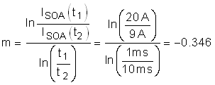
Equation 15. LM5069 Equation14_SNVS452.gif
Equation 16. LM5069 Equation15_SNVS452.gif
Equation 17. LM5069 Equation16_SNVS452.gif
Equation 18. LM5069 Equation17_SNVS452.gif

Note that the SOA of a MOSFET is specified at a case temperature of 25°C, while the case temperature can be much hotter during a hot-short. The SOA must be derated based on TC,MAX using Equation 19.

Equation 19. LM5069 Equation18_SNVS452.gif
Equation 20. LM5069 Equation19_SNVS452.gif

Based on this calculation the MOSFET can handle 7.55 A, 30 V for 7.06 ms at elevated case temperature, and is required to handle 1.25 A during a hot-short. This means the MOSFET is not at risk of getting damaged during a hot-short. In general, TI recommends for the MOSFET to be able to handle a minimum of 1.3× more power than what is required during a hot-short to provide margin to cover the variance of the power limit and fault time.