JAJSGX1G September   2006  – Jaunuary 2020 LM5069

PRODUCTION DATA.  

  1. 特長
  2. アプリケーション
  3. 概要
    1.     Device Images
      1.      代表的なアプリケーションの図
  4. 改訂履歴
    1.     Device Comparison
  5. Pin Configuration and Functions
    1.     Pin Functions
  6. Specifications
    1. 6.1 Absolute Maximum Ratings
    2. 6.2 ESD Ratings
    3. 6.3 Recommended Operating Conditions
    4. 6.4 Thermal Information
    5. 6.5 Electrical Characteristics
    6. 6.6 Typical Characteristics
  7. Detailed Description
    1. 7.1 Overview
    2. 7.2 Functional Block Diagram
    3. 7.3 Feature Description
      1. 7.3.1 Current Limit
      2. 7.3.2 Circuit Breaker
      3. 7.3.3 Power Limit
      4. 7.3.4 Undervoltage Lockout (UVLO)
      5. 7.3.5 Overvoltage Lockout (OVLO)
      6. 7.3.6 Power Good Pin
    4. 7.4 Device Functional Modes
      1. 7.4.1 Power Up Sequence
      2. 7.4.2 Gate Control
      3. 7.4.3 Fault Timer and Restart
      4. 7.4.4 Shutdown Control
  8. Application and Implementation
    1. 8.1 Application Information
    2. 8.2 Typical Application
      1. 8.2.1 48-V, 10-A Hot Swap Design
        1. 8.2.1.1 Design Requirements
        2. 8.2.1.2 Detailed Design Procedure
          1. 8.2.1.2.1 Select RSNS and CL setting
          2. 8.2.1.2.2 Selecting the Hot Swap FET(s)
          3. 8.2.1.2.3 Select Power Limit
          4. 8.2.1.2.4 Set Fault Timer
          5. 8.2.1.2.5 Check MOSFET SOA
          6. 8.2.1.2.6 Set Undervoltage and Overvoltage Threshold
            1. 8.2.1.2.6.1 Option A
            2. 8.2.1.2.6.2 Option B
            3. 8.2.1.2.6.3 Option C
            4. 8.2.1.2.6.4 Option D
          7. 8.2.1.2.7 Input and Output Protection
          8. 8.2.1.2.8 Final Schematic and Component Values
        3. 8.2.1.3 Application Curves
  9. Power Supply Recommendations
  10. 10Layout
    1. 10.1 Layout Guidelines
      1. 10.1.1 PC Board Guidelines
      2. 10.1.2 System Considerations
    2. 10.2 Layout Example
  11. 11デバイスおよびドキュメントのサポート
    1. 11.1 デバイス・サポート
      1. 11.1.1 開発サポート
    2. 11.2 ドキュメントのサポート
      1. 11.2.1 関連資料
    3. 11.3 ドキュメントの更新通知を受け取る方法
    4. 11.4 コミュニティ・リソース
    5. 11.5 商標
    6. 11.6 静電気放電に関する注意事項
    7. 11.7 Glossary
  12. 12メカニカル、パッケージ、および注文情報

Option A

The configuration shown in Figure 30 requires three resistors (R1-R3) to set the thresholds.
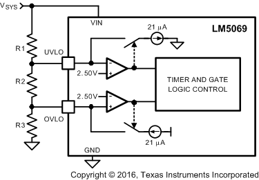
LM5069 20197229.gifFigure 30. UVLO and OVLO Thresholds Set By R1-R3

The procedure to calculate the resistor values is as follows:

  1. Choose the upper UVLO threshold (VUVH), and the lower UVLO threshold (VUVL).
  2. Choose the upper OVLO threshold (VOVH).
  3. The lower OVLO threshold (VOVL) cannot be chosen in advance in this case, but is determined after the values for R1-R3 are determined. If VOVL must be accurately defined in addition to the other three thresholds, see Option B below.

The resistors are calculated with Equation 21, Equation 22, and Equation 23.

Equation 21. LM5069 20197230.gif
Equation 22. LM5069 20197231.gif
Equation 23. LM5069 20197232.gif

The lower OVLO threshold is calculated from Equation 24.

Equation 24. LM5069 20197233.gif

As an example, assume the application requires the following thresholds: VUVH = 36 V, VUVL = 32 V, VOVH = 60 V.

Equation 25. LM5069 20197234.gif
Equation 26. LM5069 20197235.gif
Equation 27. LM5069 20197236.gif

The lower OVLO threshold calculates to 55.8 V, and the OVLO hysteresis is 4.2 V. Note that the OVLO hysteresis is always slightly greater than the UVLO hysteresis in this configuration. When the R1-R3 resistor values are known, the threshold voltages and hysteresis are calculated from Equation 28 through Equation 33.

Equation 28. LM5069 20197237.gif
Equation 29. LM5069 20197238.gif
Equation 30. VUV(HYS) = R1 × 21 µA
Equation 31. LM5069 20197239.gif
Equation 32. LM5069 20197240.gif
Equation 33. VOV(HYS) = (R1 + R2) × 21 µA